General Question
athavan-mahen opened this issue · 8 comments
Hi this is going to be my first project so i have some questions
1, can i download the USB diagram so i can edit them
2, when you order it from dirtypcbs and when then ship it do they cut the excess board so it fits in the USB port and the keyhole already punched out or do we need to cut them
3, what is the difference between Non-panelized and panelized
Thank you in advance for answering my question
-
USB diagram?
-
Yes they will cut it according to how it is drawn in the gerbers, which is what is posted in the releases. Keyhole is cut out.
-
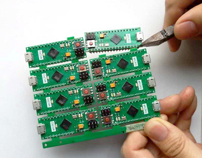
Here is a picture of a panelized set of PCBs
And here is panelized U2F Zero's. You get three on the same die instead of the non panelized one.

hi conorpp
thanks for the fast reply what I meant by the USB diagram is the file name "u2f-zero-gerbers.zip" so i can try to make some changes
Thank you in advance for the reply
Hi rickard-von-essen
Thank you for the fast message, I really appreciate it as this help me to get a visual of the printed board
Thank you
You can use Kicad to edit the PCB layout and regenerate the gerbers
Hi Conorpp where can I download the file for the PCB so I can edit them '
Thanks you
You can download the source using git or just download everything as a zip from the repo page.
Then open "hardware/u2f-zero.pro" in Kicad.
Hope you got everything you needed, feel free to email me if you have more questions.