The main purpose of this project is to get an insight into the STM32F407 Discovery Board, which is an ARM Cortex M4 based Microcontroller. As I started working on STM32F07 Discovery Board, initially it was difficult and confusing to understand and program this microcontroller because understanding internal structures and working of the microcontroller using datasheet of STM32F407VGT MCU is difficult especially if one is a beginner.
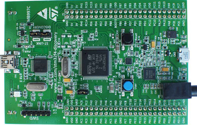
Figure 1 : STM32F407 Discovery Board
This project gives almost all the basic information needed to get started with STM32F407 Discovery Board and also development of driver code.
Hardware Used : STM32F4 DISCOVERY kit, for more information visit https://www.st.com/en/evaluation-tools/stm32f4discovery.html
Software Tool : Kiel MDK V5, for more information visit http://www2.keil.com/mdk5/. For installation of Keil MDK V5, refer https://youtu.be/d_O2tu5CMbQ
Note : As this microcontroller has many advanced features and the main aim of this project is to get all basic insights, during the driver development only the required functionalities are added and other advanced functionality is not added. I may update the driver and other functionality in the future.
Please find the STM32F4 Discovery User Manual,STM32F4xxx Reference Manual (RM0090) and other related documents inside a folder called Documents. I will be referring to these documents for information such as block diagrams, register details ect.
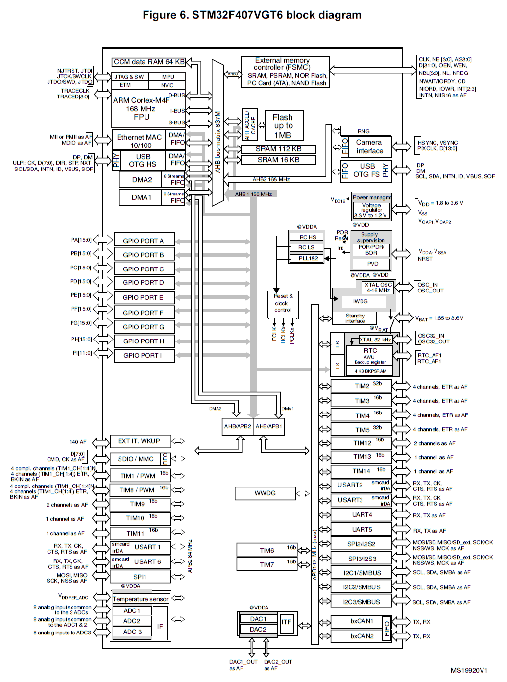
Please refer : Figure 6. STM32F407VGT6 block diagram from 'STM32F4 Discovery User Manual' (Page 12).
The STM32F407 Discovery board uses STM32F407VGT6 Microcontroller which has ARM Cortex-M4F Processor, which is capable of running upto 168Mhz. This MCU has many peripherals such as GPIO ports, TIMERS, ADCs, DACs, Flash Memory, SRAM, SPI, UART ect. The processor and peripherals talk via BUS-Interface. There are three busses available :-
- I-BUS (Instruction Bus)
- D-BUS (Data Bus)
- S-BUS (System Bus)
I-BUS This bus connects the Instruction bus of the Cortex®-M4 with FPU(Floating point unit) core to the BusMatrix. This bus is used by the core to fetch instructions. The target of this bus is a memory containing code (internal Flash memory/SRAM or external memories through the FSMC/FMC).
D-BUS This bus connects the databus of the Cortex®-M4 with FPU to the 64-Kbyte CCM data RAM to the BusMatrix. This bus is used by the core for literal load and debug access. The target of this bus is a memory containing code or data (internal Flash memory or external memories through the FSMC/FMC).
S-BUS This bus connects the system bus of the Cortex®-M4 with FPU core to a BusMatrix. This bus is used to access data located in a peripheral or in SRAM. Instructions may also be fetched on this bus (less efficient than ICode). The targets of this bus are the internal SRAM1, SRAM2 and SRAM3, the AHB1 peripherals including the APB peripherals, the AHB2 peripherals and the external memories through the FSMC/FMC.
So instructions and data use I-bus and D-bus respectively, All the other peripheral uses System bus. The Cortex-M4 processor contains three external Advanced High-performance Bus (AHB)-Lite bus interface and one Advanced Peripheral Bus (APB) interface. The GPIOs are connected to AHB1 bus which has a maximum speed of 150Mhz and is divided into two buses as APB1 and APB2. APB1 runs at 42Mhz(max) and APB2 runs at 82Mhz(max). The different peripherals such as SPI, UART, TIMERs, ADCs, DACs, etc are connected to either APB1/APB2 buses. And the AHB2(168Mhz max) is connected to Camera and USB OTG interfaces, AHB3 is connected to External memory controller.
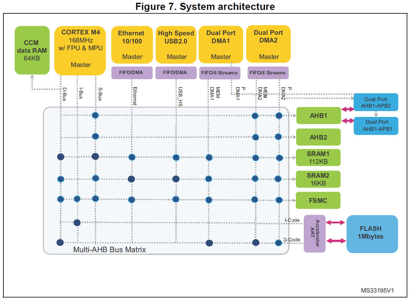
Please refer : Figure 7. System architecture from 'Using the STM32F2 and STM32F4 DMA controller(AN4031)' (page 18).
Refering to the figure 7, The Yellow blocks are Master and blocks in Green are Slaves, there are lots of connected dots which actually says that there is path from master to slave for communication. In Microcontroller , the communication between the processors and the peripherals is seen in the scope of communication between master and slave. Here the processor ARM Cortex-M4 itself is a master, and it may have other masters such as Ethernet, High Speed USB 2.0, DMA1 and DMA2.
STM32F407VGT6 Micorcontroller has 3 main clock sources:
-
Crystal Oscillator(HSE) - This is external clock source which can be connected to MCU based on requirements. HSE standas fro High speed External. If you want to use HSE as system clock an external crystal oscillator(whose frequency must be in range 4 to 26Mhz ) has to be connected. In this board, the manufacturer has connected 8Mhz crystal.
-
RC Oscillator (HSI) - All modern MCU comes with internal RC Oscillator, which can be just activated to use. HSI stands for High Speed Internal .After Reset, by default HSI is used to provide a clock to MCU, which means by default MCU select HSI as the clock. This clock is internal to MCU and its value is 16Mhz in STM32F407 MCU. The HSI internal oscillator has the advantage of providing a clock at a low cost, as no external component is required to use this clock. It also has a faster start-up time than the external crystal oscillator however, frequency is less accurate when compared to the external crystal oscillator.
-
PLL(Phase locked loop) - It is also Implemented internally in MCU, it uses low frequency sources to generate high frequency clock (PLLCLK).The power of PLL lies in producing high-frequency clocks of various programmable range. By using PLL you can boost the HCLK(AHB) up to 168Mhz in STM32F4xx MCU. All the modern MCU has PLL. If you want to use MCU-buses at their maximum speed then we have to use PLL only. You have to feed either HSI or HSE to the PLL as input frequency. Then by using all PLL circuitry settings, it produces a PLL output clock in the range of 100's of Mhz. So to Run STM32F407 at its maximum frequency(168Hhz) you have to use PLL.
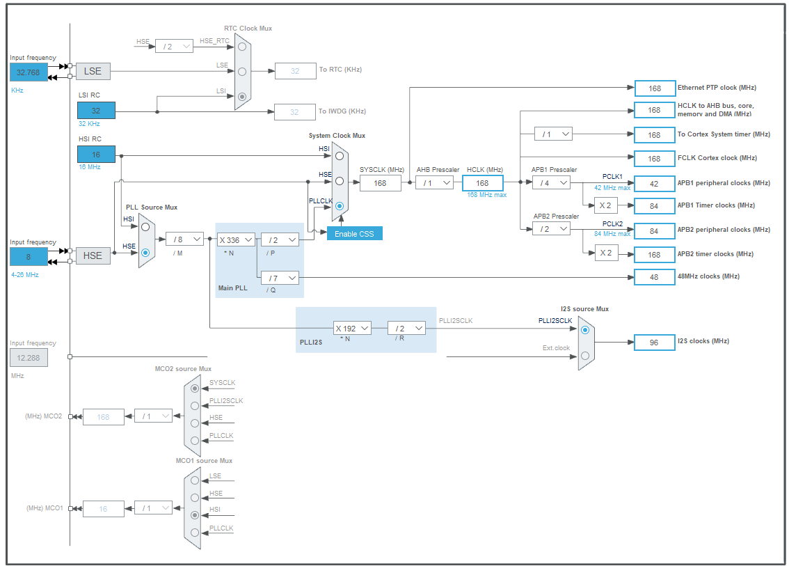
Please refer : Figure 21. Clock tree from 'STM32F4xxx Reference Manual (RM0090)' (Page 216).
Note : If your using STM32 CUBE MX tool, then select STM32F407 board and goto clock configuration for a much better clock tree representation.(I prefer to use this clock representation for easier understanding).
From above clock tree we can see that HSI RC is 16Mhz internal Clock, and an external oscillator (4Mhz to 26Mhz) has to be connected to HSE input and PLL takes HSI/HSE as input to produce various other clocks. All 3 of these clock sources are given to SYSTEM CLOCK MULTIPLEXER where we can select clock source, Output of this MUX is SYSCLK(i.e, System Clock).
- SYSCLK : This is the Main clock of MCU, using this other clocks are derived (Ex: Peripheral, Bus clocks ect). SYSCLK is given directly to Ethernet PTP Clock.
- HCLK : HCLK is derived from SYSCLK with a Prescaler in between , which brings down the clock frequency. HCLK goes directly to AHB bus, core, memory and DMA. HCLK goes to Cortex System Timer with prescalar in between and HCLK goes directly to Cortex Processor (FCLK Cortex Clock).
- PCLK : PCLK1 and PCLK2 are derived from HCLK, PCLK1 goes to APB1 peripheral clock and APB1 Timer Clock and PCLK2 goes to APB2 peripheral clock and APB2 Timer Clock.
By default MCU uses HSI (i.e internal RC Oscillator) as SYSCLK, Which means after reset HSI is used as SYSCLK Source. Before using any peripheral its clock should be enabled. Referring MUC Block Diagram, all different peripheral drives the clock from bus which it is connected. By default almost all the peripheral are deactive, which means there clocks are not enabled. RCC(Reset and clock Control) engine of MCU gives various registers to enable and disable various peripheral clocks. For more information refer RCC section of STM32F4xxx Reference Manual (RM0090), page-213.
As explained before, you can connect (4 to 26Mhz) crystal oscillator to MCU. In STM32 board manufacturer has connected 8Mhz Crystal. Even though it is connected its useless as its disabled. Before using an external oscillator, we need to enable it by using RCC Clock Control Register(RCC_CR). Refer 7.3.1 RCC clock control register (RCC_CR) (page 224 of RM0090). Referring to the RCC_CR Register:
- Bit 17 and 16 are HSERDY and HSE ON respectively
- To enable HSE, HSEON bit is made 1, then you have to wait until the HSERDY flag becomes 1, which indicates the HSE oscillator is ready to use. It important to wait until HSERDY flag is set.
- Now HSE is ready but it is not yet set as SYSCLK(System Clock).
So to set HSE as System clock, RCC clock configuration register (RCC_CFGR) is used. Refer 7.3.3 RCC clock configuration register (RCC_CFGR)(page 228 of RM0090). Referring RCC_CFGR, bit 0 and 1 are used to switch system clock.
- If Bit1:0 SW = 01, then HSE oscillator selected as the system clock .
- Once we do this HSE will be used as a system clock
It is a table of Vectors. Generally, Vectors are related to directions. We know that VECTORS in physics has both magnitude and direction. In our context we can compare pointers and direction, as pointers will point to certain addresses. So we can say that Vector table is a table which holds the specific addresses. It contains the addresses of Exception Handlers. Here system exceptions(these are MCU internally generated) and Interrupts(Which are external) are collectively called as exceptions.
Referring : Table 61. Vector table for STM32F405xx/07xx and STM32F415xx/17xx (Page 372 of RM0090)
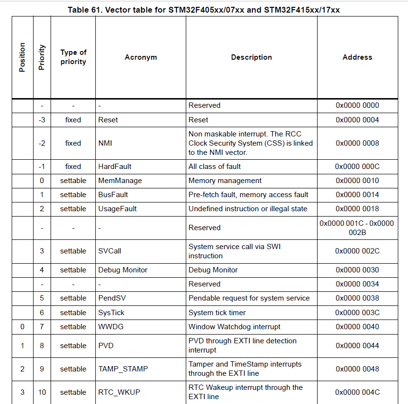
- Position: We can see that position is kept empty for all the system exceptions, system exceptions come from the processor end and vendor ST does not have control over system exceptions. These positions are with respect to NVIC(Nested vectored interrupt controller). For example, Window Watchdog interrupt is at Position 0 w.r.t to NVIC. Another name for the position is IRQ Number.
- Priority: This column gives the priority of exceptions and interrupts. From the table, we can see that Reset has the highest priority of -3.
- Type of Priority: This column tells us that whether the priority of exceptions can be changed or not. Here Reset, NMI and Hard Fault has fixed priority type and the remaining exceptions have settable priority type which means its priority can be changed.
- Address: This column tells that where exactly in the processor memory map you have to keep the corresponding exception handler. A handler is just a C function which takes care of that exception. for example, if we have implemented a function to handle NMI exception in your program then address of that handler must be kept at 0x0000 0008, that is function pointer should be kept in this addresses. The very first address that is 0x00000000 is reserved and it has special data known as STACK Pointer value in Cortex Processor. Before coming to the Reset handler, the processor loads the value stored in 0x00000000 location into stack pointer. Because always stack pointer must be initialized before entering into any handler. So we must keep a valid value at this address. All these initializations are handled in startup code.
Interrupts are a common feature supported by almost all microcontrollers. They are typically generated by hardware, for example peripherals or external input pins. When a peripheral or hardware needs service from the processor, this will lead to changes in program flow control outside the normal programmed sequence. Typically, the following sequences would occur:
- The peripheral asserts an interrupt request to the processor.
- The currently running task is suspended by the processor.
- The processor executes an Interrupt Service Routine (ISR) to service the peripheral, and optionally the interrupt request is cleared by software if needed.
- The processor resumes the previously suspended task. For every interrupt there must be a program associated with it. When an interrupt occurs, this program is executed to perform certain service for the interrupt. This program is usually named as Interrupt Service Routine (ISR) or interrupt handler.
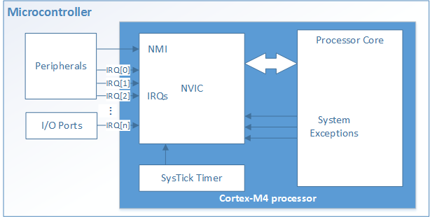
As the above figure shows every Cortex-M4 processor provides a Nested Vectored Interrupt Controller (NVIC) for interrupt handling. NVIC facilitates low-latency exception and interrupts handling, controls power management and implements System Control Registers. The NVIC and the processor core interface are closely coupled, which enables low latency to interrupt processing and efficient processing of late arriving interrupts.
For this microcontroller, the NVIC receives interrupt requests from various sources. In addition to interrupt requests, ther are some other events which need servicing. They are called “exceptions” (which are MCU internally generated). For Cortex-M4 processor, exceptions include resets, software interrupts and hardware interrupts. Each exception has an associated 32-bit vector that stores the memory location where the ISR that handles the exception is located. These vectors are stored in ROM at the beginning of memory. As explained earlier Vector table holds the location of ISR. The Cortex-M4 NVIC supports up to 240 interrupt requests (IRQs), a non-maskable interrupt (NMI), a SysTick timer interrupt and a number of system exceptions. Most of these IRQs are generated by peripherals such as timers, GPIO ports and communication interfaces such as UARTs.
We can observe that not all interrupts go directly to NVIC. Some peripheral deliver their interrupt to NVIC over the EXTI Lines and Some peripheral deliver their interrupts directly to NVIC. This is the design of STM.
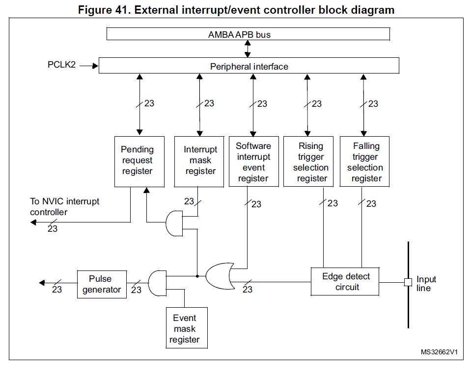
Refer: Figure 41. External interrupt/event controller block diagram (Page 380 of RM0090)
STM MCU has an engine called EXTI(External interrupt/event Controller). This engine is hanging on APB2 bus, so it drives the clock from PCLK2. This engine is finally connected to NVIC Interrupt Controller. This engine gives 23 lines to NVIC. In the vector table, we can see 23 entries related to EXTI.
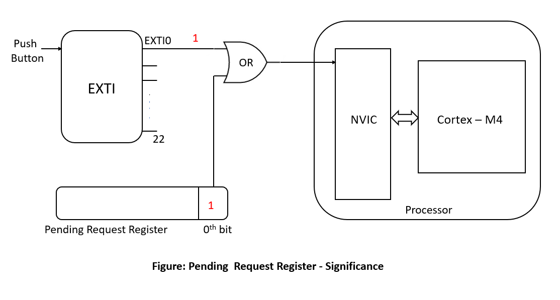
In EXTI it is important to know about Pending Request Register. This Register tells us on which EXTI line an interrupt is pending. When an interrupt occurs corresponding bit in this register goes high. Once the interrupt event is finished, its programmer responsibility to clear this bit. If the bit is not cleared it leads to a bug. For instance consider that when a push-button is pressed an interrupt is generated, this interrupt is given to NVIC via EXTI0 Line as shown below in the figure: Pending Request register Significance.
So when the push-button is pressed, EXTI0 line goes high and also a corresponding bit in pending request register goes high. So both input to the OR gate is one hence an interrupt is triggered on NVIC. If we do not clear this bit in pending request register after the event is finished EXTI0 goes low but one of input to OR gate remains high due to pending request register so even though an interrupt event is completed an interrupt is continuously triggered in NVIC which leads to a problem. So it is important to clear this bit after the interrupt event is completed.
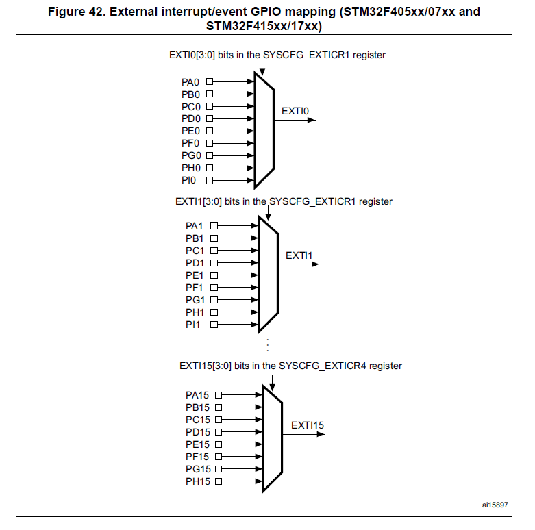
Refer: Figure 42. External interrupt/event GPIO mapping (STM32F405xx/07xx and STM32F415xx/17xx) (Page 382 of RM0090)
Figure 42 shows how exactly the GPIOs are delivering their interrupts to NVIC. The 168 GPIOs are connected to the 16 external interrupt/event lines as shown above. All the 0th Pins (PA0, PB0, PC0, PD0, PE0, PF0, PG0, PH0, and PI0) of GPIO ports are connected to EXTI0 line through MUX, In a similar way from figure42, we can see that how remaining pins deliver their interrupts. The EXTI0[3:0] bits in the SYSCFG_EXTICR1 register is used to select the source input for the EXTIx external interrupt.
- GPIO - General Purpose Input and Output
- SPI - Serial Peripheral Interface]
- USART/UART - Universal Synchronous/Asynchronous Receiver Transmitter
- I2C - Inter-Integrated Circuit
