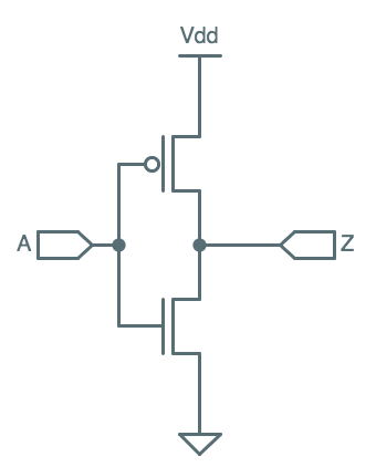
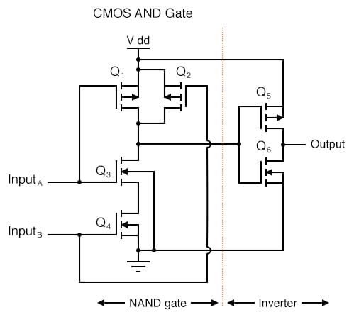
Repository of Schematic diagram , SSI layout , simulation graph of Logic gates and IC
Basically I am using Electric VLSI design system to design Logic gates and IC's schematic diagram and layouts.
I always simulate all the things in LTSpice XVII software to get or check the output is correct or not.
N.B : Make sure that you have installed Jdk first. Electric VLSI needs java run time Environment to operate.
I will update this repository as soon as possible.
If you want to know about NOR gate click here
layout design of NOR gate (Electric vlsi)
Simulation of NOR gate (LTSpice XVII)
During this Simulation you need to provide input signal or spice code this code is here,
vdd vdd 0 DC 5
va A 0 DC pwl 10n 0 20n 5 50n 5 60n 0 90n 0 100n 5 130n 5 140n 0 170n 0 180n 5
vb B 0 DC pwl 10n 0 20n 5 100n 5 110n 0
.measure tran tf trig v(AnorB) val=4.5 fall=1 td=4ns trag v(AnorB) val=0.5 fall=1
.measure tran tr trig v(AnorB) val=0.5 rise=1 td=4ns trag v(AnorB) val=4.5 rise=1
.tran 200n
.include D:\Electric\projects\C5_models.txtIf you want to know about NOR gate click here
.png?raw=true&raw=true)
layout design of NOT gate (Electric vlsi)
.png?raw=true&raw=true)
simulation of NOT gate (LTSpice XVII)
spice code
vdd vdd 0 DC 5
vin A 0 pulse 5 0 0 300n 300n 2u 4u
.trans 10u
.include D:\Electric\projects\C5_models.txtIf you want to know about NAND gate click here
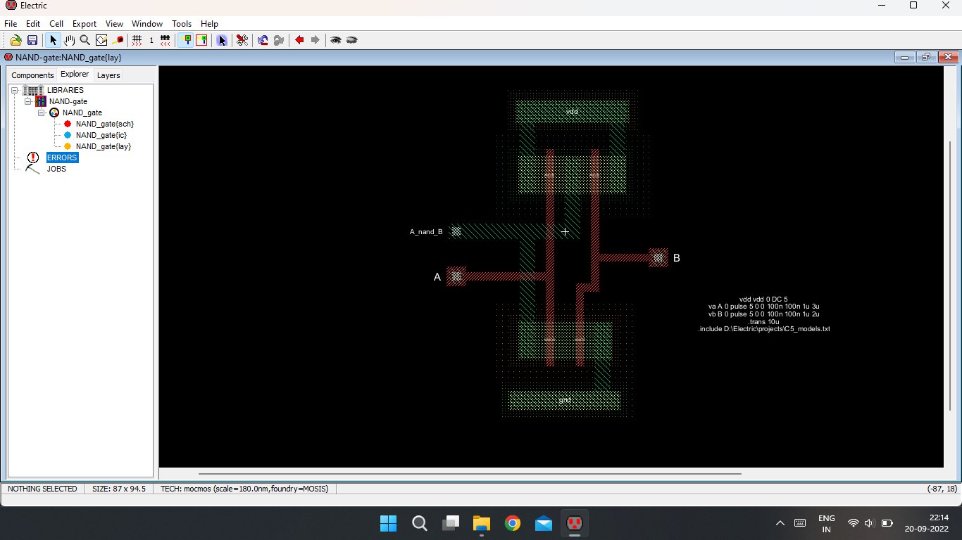
layout design of NAND gate (Electric vlsi)
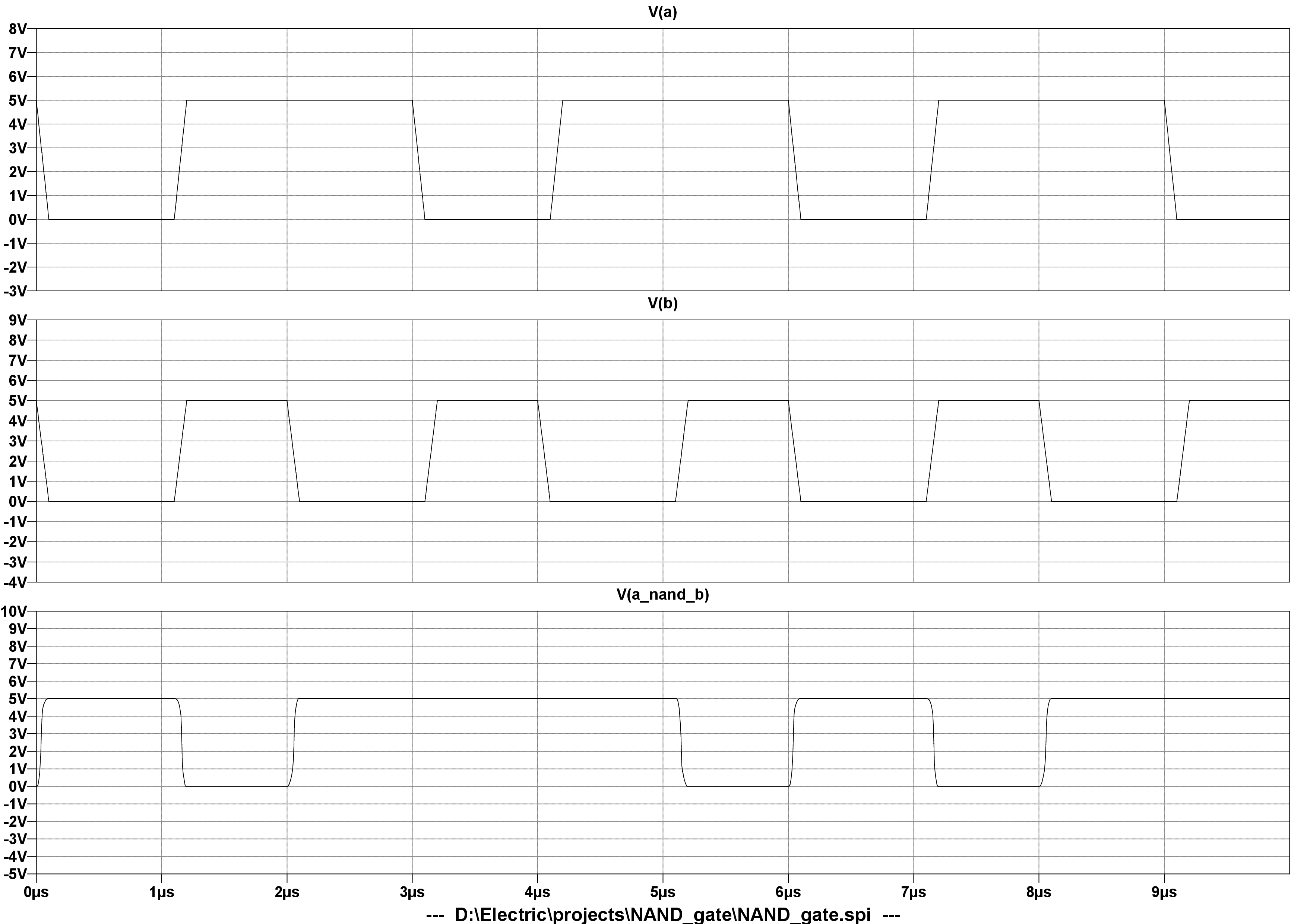
simulation of NAND gate (LTSpice XVII)
spice code
vdd vdd 0 DC 5
va A 0 pulse 5 0 0 100n 100n 1u 3u
vb B 0 pulse 5 0 0 100n 100n 1u 2u
.trans 10u
.include D:\Electric\projects\C5_models.txtIf you want to know about AND gate click here
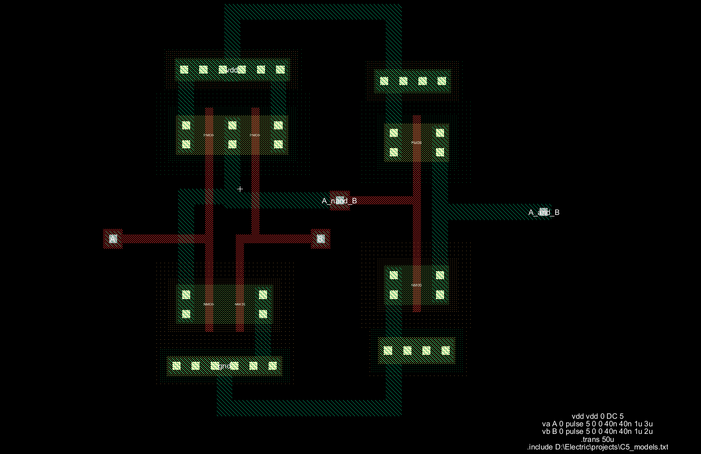
layout design of AND gate (Electric vlsi)

simulation of AND gate (LTSpice XVII)
spice code
vdd vdd 0 DC 5
va A 0 pulse 5 0 0 40n 40n 1u 3u
vb B 0 pulse 5 0 0 40n 40n 1u 2u
.trans 50u
.include D:\Electric\projects\C5_models.txt
If you will face any type of problems, feel free to ask
And
Be aware from layout shorts and DRC-ERC errors.😁

.png)
.png)
