![]()
![]()
![]()
This is a submission for TinyTapeout 2.
Author's note: I thought I'd give this a bit of a nostalgic feel by calling it the '5401', like it's some old microprocessor from the 70s or 80s. Of course had to be complete with a made-up brand name, which is where the 'Avalon Semiconductors' comes from. Documentation for this is quite long, but I hope it will be a informative as well as enjoyable read.
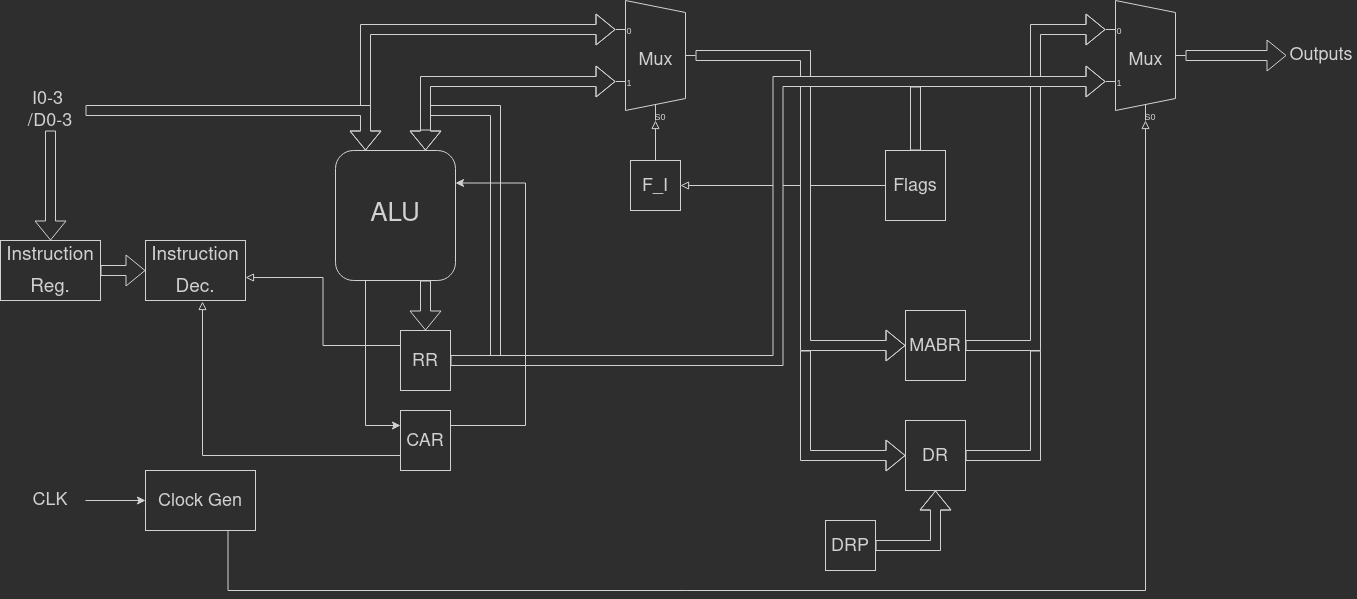
The 5401 is a 4-bit hybrid Harvard architecture microprocessor capable of addressing up to 4096 bytes of program memory, and 249 words of data memory. This is possible through multiplexing on both the input and output ports. The processor also contains hardware multiply and divide units, as well as 10 words of on-chip RAM and general-purpose inputs, accessible through special memory addresses.
| Inputs | --- | Outputs |
|---|---|---|
| CLK - | - MAR0 / DR0 / DR8 / RR0 | |
| RST - | - MAR1 / DR1 / DR9 / RR1 | |
| I0 / D0 - | - MAR2 / DR2 / DR10 / RR2 | |
| I1 / D1 - | - MAR3 / DR3 / DR11 / RR3 | |
| I2 / D2 - | - MAR4 / DR4 / F_MAR | |
| I3 / D3 - | - MAR5 / DR5 / F_WRITE | |
| EF0 - | - MAR6 / DR6 / F_JMP | |
| EF1 - | - MAR7 / DR7 / F_I |
| Name | Description |
|---|---|
| CLK | Clock input |
| RST | Reset input |
| I0 - I3 | Instruction input |
| D0 - D3 | Data input |
| EF0 - EF1 | Event flag general-purpose inputs |
| MAR0 - MAR7 | New value of Memory Address Register, valid when F_MAR = 1 |
| DR0 - DR11 | Value of Destination Register, to be loaded into PC when F_JMP = 1 |
| RR0 - RR3 | Value of Result Register, to be written to memory when F_WRITE = 1 |
| F_MAR | MAR-flag, indicating the processor wants to update the Memory Address Register |
| F_WRITE | WRITE-flag, indicating a memory write |
| F_JMP | JUMP-flag, indicating the processor wants to set the PC to a new value |
| F_I | I-flag, indicating the processor wants the next instruction to receive data from program memory rather than data memory |
The 5401 internally operates on a two-phase clock, requiring 4 clock cycles to execute each instruction, named T0 - T3. The external control logic must be capable of counting which cycle it is on, as the outputs of the processor can only be latched or acted upon in certain states. Additionally, the 5401 does not include a program counter, or address register. Both must be implemented by the control logic. The processor is, however, capable of buffering and providing new values for these registers.
The following table contains descriptions of each clock phase, and how the control logic must act in each state.
| Clock state | Description |
|---|---|
| T0 | Rising edge of first internal clock phase. Control logic must be in a stable state, and be providing an instruction to the processor on the rising edge of this cycle. The control logic must switch from providing an instruction to providing data on the falling edge of this cycle. |
| T1 | Falling edge of the first internal clock phase. Control logic must latch all 8 output ports on the falling edge of this cycle. |
| T2 | Rising edge of second internal clock phase. No change in control logic. |
| T3 | Falling edge of second internal clock phase. Control logic must sample the states of the status bits and act upon any active flags on the falling edge of this cycle, and the I-flag must be latched. The Program Counter can safely be incremented on the falling edge of this cycle, and the control logic can switch to providing the next instruction. |
The data provided to the processor after the falling edge of T0 should, by default, come from data memory at the address pointed to by the Memory Address Register. This behaviour should only be overriden by the I-flag.
The data byte emitted on the falling edge of T1 may be called "DB0", while the data byte emitted on the falling edge of T3 may be called "DB1"
Upon detection of an active flag, the control logic must respond to it on the falling edge of T3. An expection to this is the I-flag, which influences the execution of the next instruction, and thus must be latched. Only one flag can ever be active at a time. It is possible for no flags to be active, in which case the control logic should take no special action.
The processor is requesting the external Memory Address Register be updated with a new value. The data byte latched during T1 is the new value to be loaded.
The processor is requesting to write to memory. The current value of the Result Register is provided on output pins 1 - 4. This value should be written to to the memory location pointed to by the Memory Address Register.
The processor is requesting the Program Counter be loaded with a new value. The least significant 8 bits of the new value are provided by the data word latched during T1, while the most significant 4 bits are provided on output pins 1 - 4. The Program Counter increment must be inhibited during this cycle.
Flag I, also called the Immediate Flag, indicates to the control logic that the next instruction wants to load from program memory, rather than data memory. The memory location to be read from is the same as the memory location of the following instruction. If a standard 8-bit ROM is used as the program memory, instructions may be stored in the lower nibble, and data in the higher nibble. This flag must be latched to take effect during the entirety of the following instruction. It must not be cleared until the next falling edge of T3 where the flag is inactive.
The following registers are present inside the 5401:
| Name | Mnemonic | Size (bits) | Description |
|---|---|---|---|
| Instruction Register | IR | 4 | Holds the instruction currently being executed |
| Result Register | RR | 4 | Accumulator register |
| Carry flag | CAR | 1 | Stores the carry bit after an addition or substraction operation |
| Destination Register | DR | 12 | Buffers the branch target for jump instructions |
| Memory Address Buffer Register | MABR | 8 | Internal buffer of the Memory Address Register |
| Destination Register Pointer | DRP | 3 | Pointer to one of the three words comprising the Destination Register |
| Factor A register¹ | FA | 4 | First factor input of the hardware multiply unit |
| Factor B register¹ | FB | 4 | First factor input of the hardware multiply unit |
| Product Register¹² | PR | 8 | Output of the multiply unit |
| Dividend Register¹ | DR | 8 | Dividend input of the hardware divide unit |
| Divisor Register¹ | DiR | 4 | Divisor input of the hardware divide unit |
| Remainder Register¹² | ReR | 4 | Remainder output of the divide unit |
| Quotient Register¹² | QR | 8 | Quotient output of the divide unit |
¹ Memory mapped
² Virtual register
Virtual registers are locations that yield data when read, but are not physically present as latches in the processor. For instance, the PR virtual register will read as the current output of the multiply unit, which is not buffered and determined by the values currently residing in the FA and FB registers.
The 5401 posseses several memory-mapped registers and devices. These are accessible by reading or writing to specific memory locations. The following addresses are reserved for this functionality:
| Address | Destination |
|---|---|
| FAh | FA (write), lower word of PR (read) |
| FBh | FB (write), upper word of PR (read) |
| FCh | Lower word of DR (write), ReR (read) |
| FDh | Upper word of DR (write), lower word of QR (read) |
| FEh | DiR (write), upper word of QR (read) |
| FFh | EF0 - EF1 (read-only) |
Locations FAh - FEh access different locations depending on the direction of the data transfer. For instance, a write to location FAh will set the value of the FA register, while a read from FAh will yield the value in the lower 4 bits of the PR register. Location FFh is read-only, and writes to this location will be discarded.
When executing a STR instruction on one of these locations, the WR flag will be supressed.
Memory locations FAh and FBh can be used to interact with the hardware multiply unit. This part of the processor will perform a multiplication on the two words stored in the FA and FB registers, outputting a 8-bit value in PR, so no part of the result is lost. The two halves of PR can be read individually from the two memory locations.
Memory locations FCh - FEh are wired to the hardware divide unit, which divides an 8-bit value by a 4-bit value. After loading DR and DiR with arguments, the 4-bit remainder of the division will be visible at ReR, and the 8-bit result at QR.
The 5401 has two, general-purpose input ports, EF0 and EF1. They are memory mapped. If the MABR is set to FFh and the LD instruction is executed, bits 0 and 1 of the loaded data word will defined by the states of EF0 and EF1. Bit 0 will be 1 if EF0 is at a high logic level (0 otherwise), while bit 1 will be 1 if EF1 is at a high logic level (0 otherwise). Bits 2 and 3 will be 0.
The 5401 has 10 words of built-in RAM, accessible at memory locations F0h - F9h. Any memory reads and writes to those addresses will be served by the internal RAM. The WRITE flag is supressed during a STR instruction on these addresses.
| Instruction | Mnemonic | Opcode | Operation |
|---|---|---|---|
| Load RR | LD | 0000 | RR = Data |
| Store RR | STR | 0001 | DB1[3:0] = RR; F_WRITE = 1 |
| Set I | SEI | 0010 | F_I = 1 |
| Load MAR Lower | LML | 0011 | IF I: MABR[3:0] = Data; ELSE: MABR[3:0] = RR; DB0 = MARB; F_MAR = 1 |
| Jump, unconditional | JMP | 0100 | DB0 = DR[7:0]; DB1[3:0] = DR[11:8]; F_JMP = 1 |
| Jump if Carry | JC | 0101 | IF CAR: DB0 = DR[7:0]; DB1[3:0] = DR[11:8]; F_JMP = 1; ELSE: nop |
| Jump if Zero | JZ | 0110 | IF RR == 0: DB0 = DR[7:0]; DB1[3:0] = DR[11:8]; F_JMP = 1; ELSE: nop |
| Load Destination Register | LDR | 0111 | IF I: DR[DRP*4+3:DRP*4] = Data; ELSE: DR[DRP*4+3:DRP*4] = RR; DRP = (DRP + 1) % 3 |
| Add to RR | ADD | 1000 | RR, CAR = RR + data |
| Substract from RR | SUB | 1001 | RR, CAR = RR - data |
| Add to RR with carry | ADC | 1010 | RR, CAR = RR + data + CAR |
| Substract from RR with carry | SUC | 1011 | RR, CAR = RR - data - ~CAR |
| Logic OR with RR | OR | 1100 | RR = RR | data |
| Logic AND with RR | AND | 1101 | RR = RR & data |
| Logic XOR with RR | XOR | 1110 | RR = RR ^ data |
| Load MAR Higher | LMH | 1111 | IF I: MABR[7:4] = Data; ELSE: MABR[7:4] = RR; DB0 = MARB; F_MAR = 1 |
This instruction will load the contents of the data bus into the Result Register.
The value of the Result Register will be written to memory.
The I-flag will be set both internally and externally. With the exception of LDR, the completion of the following instruction will automatically clear the flag. It also modified the behaviour of the LML, LMH and LDR instructions.
These instructions will set one nibble of the Memory Address Register at a time. Both instructions write to the Memory Address Buffer Register first, before the full contents of this register are sent out to the control logic, to become the new value of the Memory Address Register. By default, both instructions will load the value of the Result Register into the MABR, but if the I-flag is set, they will instead fetch a value from the data bus, allowing constant values to be loaded.
This group of instructions will take the contents of the Destination Register, and send them out to the control logic to become the new Program Counter value, effectively moving program execution to a new location. JC and JZ do this conditionally, with the instruction being skipped if their condition is not met. JC will check the current value of the Carry Flag, and not branch if it is 0, and JZ will check the current value of the Result Register, and only branch of it is equal to 0.
Part of the value of the Destination Register will be loaded. As the Destination Register is 12 bits wide, it cannot be loaded all at once. Instead, it is segmented into three words of 4 bits each. A pointer is stored in the Destination Register Pointer register, pointing to one of these three words. The word currently pointed to by the DRP will be set, and the DRP is advanced. The DRP cycles back around to 0 after the third word has been written. A full load of the entire Destination Register thus requires three executions of the LDR instruction. By default, the instruction will load the value of the Result Register into the DR, but if the I-flag is set, it will instead fetch a value from the data bus, allowing constant values to be loaded. Additionally, this instruction will inhibit the I-flag from being reset at its completion, meaning the flag stays active for the next instruction. This allows the entire DR to be rapidly loaded with constant data by executing SEI once, followed by three times LDR.
A value from the data bus will be added onto the Result Register. The carry flag will be set if the result overflows the RR, but cleared otherwise. In the case of ADC, the previous carry flag will also be added onto the result.
A value form the data bus will be substracted from the Result Register. The carry flag will be cleared if the result underflows the RR, but set otherwise. In the case of ADC, the inverse of the previous carry flag will also be substracted from the result.
A logical operation will be performed between the Result Register and a value from the data bus. The carry flag will not be updated.
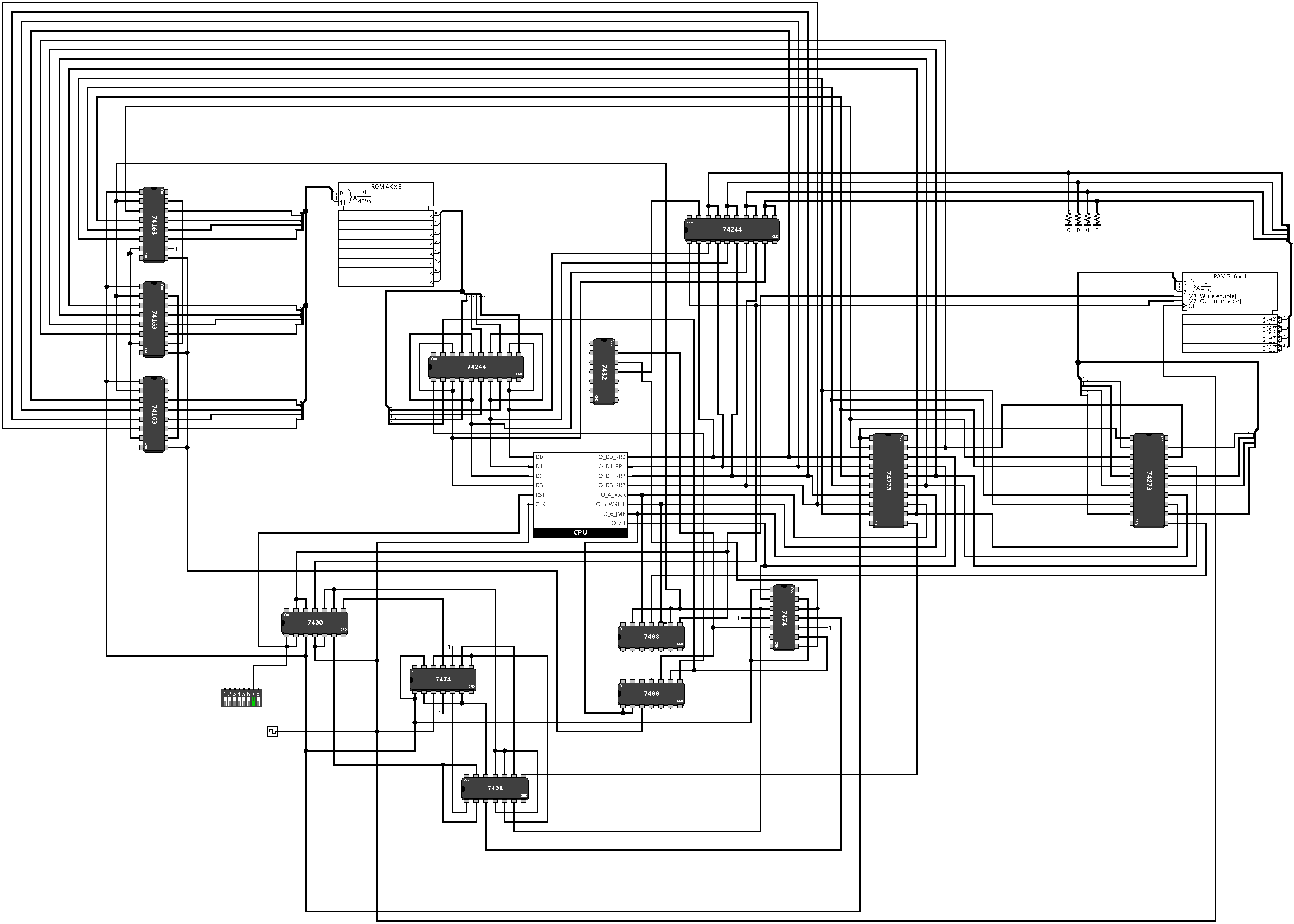
This circuit diagram shows a functional computer using the 5401 capable of executing all instructions as intended. It is implemented using only 74-series logic, though the design could be simplified through the use of a GAL.