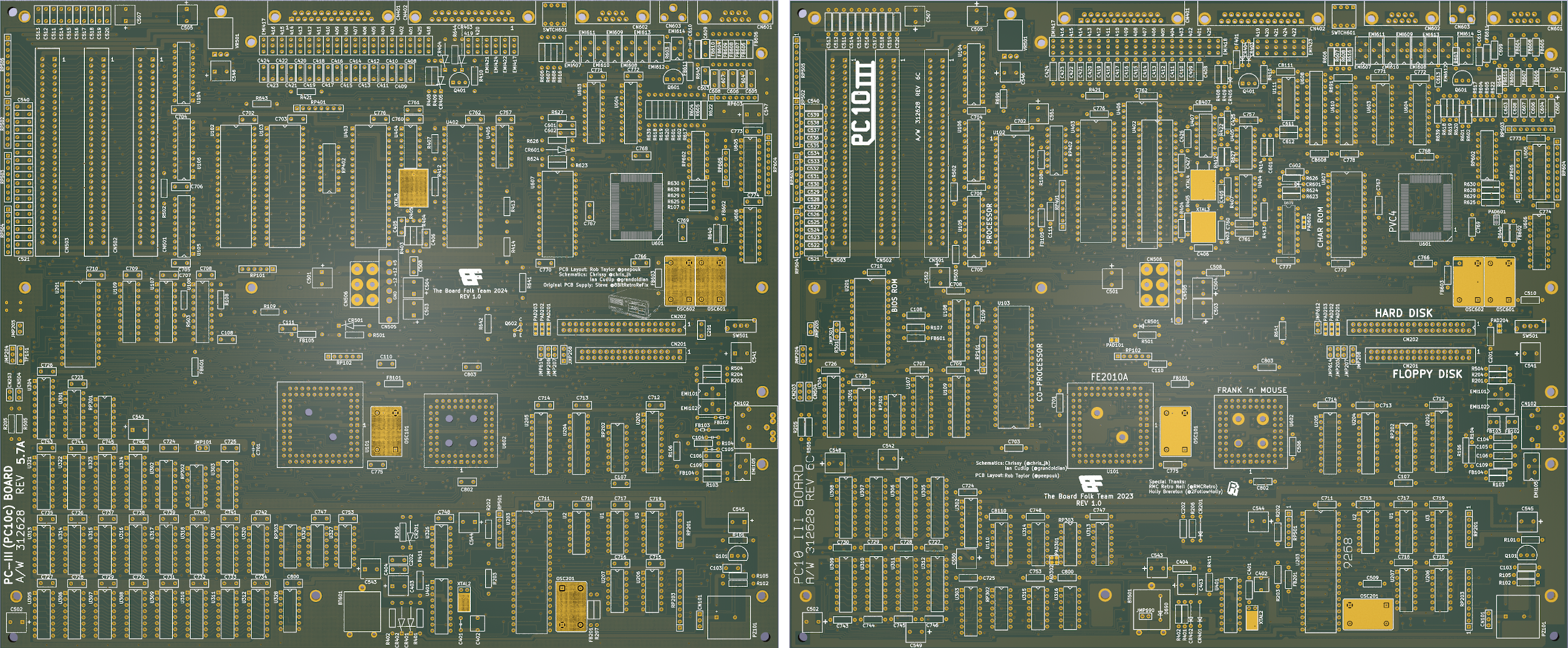
This repository contains a recreation of the main board PCB for Commodore PC10-III 312628 Revisions 5.7A and 6c. This recreation is based on the available schematics for the Commodore PC10-III and reverse engineering using scanned images of the original board's copper layers, so should be a reasonably accurate reproduction.
-
JMP690 & D690 - External Rechargable Battery Connection. Diode is for overcharging protection to a Lithium battery. Search Amazon for a lithium rechargeable battery 3.7v 2 pin header. The External connector Pin 1 GND, Pin 2 +5v (next to the diode)
-
The original board had some bodge wires and resistors. This Reproduction has them built in.
Minimum track widths, clearances and via sizes are within the standard offering of modern PCB fabricators. Gerber files are provided to the specification of JLCPCB, but should also work with PCBWay see below links to shared products.
The design is verified to work as a 2-layer PCB.
ENIG is recommended, but HASL will work also.
Most parts are marked on the board and it is expected that these will be reused from a donor board. It is completely possible that your particular board uses different (but compatible) parts so it's advisable to take photos before starting.
- Rob Taylor (@PeepoUK) for doing most of the PCB layout
- Ian Cudlip (@grandoldian) Schematics
- Chrissy (@chris-jh) Schematics
- Steve (@8BitRetroFix) provided 5.7a PCB
- RMC Retro (@RMCRetro) provided 6c PCB
- The rest of the Board Folk Team for their support and general
coolness.
As the product of this project is a replica of a proprietary product, the the author makes no claim of copyright to the schematics nor PCB layouts and releases these into the public domain, solely for the purposes of study and historical preservation.
You are free to produce PCBs based on this project's designs at your own risk and without limitation, for your own use or for sale and/or repair at a reasonable price. Attribution is appreciated. The authors are not obliged to provide support of any kind.
Under no circumstances will the authors be held responsible or liable in any way for losses, damages or costs resulting from the use of the information and/or resources of this project.
The resources are provided "as-is" without warranty of any kind, either expressed or implied, including, but not limited to, the implied warranties of merchantability and fitness for a particular purpose.

