- Introduction
- Processor Features
- Differences to the Original MSP430 Processors
- Implementation Results
- Performance
- Quick Start
- Change Log
- Contact
- Disclaimer, Proprietary and Legal Notice
Welcome to The NEO430 Processor project!
You need a small but still powerful, customizable and microcontroller-like processor system for your next FPGA project? Then the NEO430 is the right choice for you.
This processor is based on the Texas Instruments MSP430(TM) ISA and provides full compatibility with the original instruction set. The NEO430 is not an MSP430 clone – it is more like a complete new implementation from the bottom up. The processor features a very small outline, already implementing standard features like a timer, a watchdog, UART, TWI and SPI serial interfaces, general purpose IO ports, an internal bootloader and of course internal memory for program code and data. All of the implemented peripheral modules are optional – so if you do not need them, you can exclude them from synthesis to reduce the size of the system. Any additional modules, which make a more customized system, can be connected via a Wishbone-compatible bus interface or directly implemented within the processor. By this, you can built a system, that perfectly fits your needs.
It is up to you to use the NEO430 as stand-alone, configurable and extensible microcontroller, or to use it as controller within a more complex SoC design.
The high-level software development is based on the free TI msp430-gcc compiler tool chain. You can either use Windows (PowerShell or Linux Subsystem) or Linux as build environment for your applications – the project supports both worlds.
This project is intended to work "out of the box". Just synthesize the test setup from this project, upload it to your
FPGA board of choice (the NEO430 uses a FPGA vendor-independent VHDL description) and start exploring the capabilities of
the NEO430 processor. Application program generation works by executing a single "make" command. Jump to the
"Let’s Get It Started" chapter in the NEO430 documentary, which provides a lot of guides and tutorials to make your first
NEO430 setup run:  NEO430 Datasheet

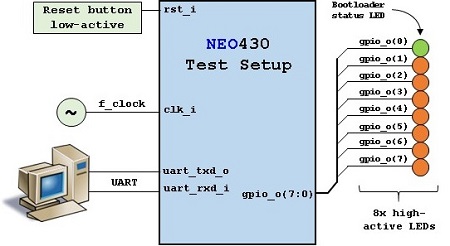
(optional modules are marked using dashed lines in the figure above)
- 16-bit open source soft-core microcontroller-like processor system
- Full support of the original MSP430 instruction set architecture
- Code-efficient CISC-like instruction capabilities
- Tool chain based on free TI msp430-gcc compiler
- Application compilation scripts (makefiles) for Windows Powershell / Windows Subsystem for Linux / native Linux
- Software requirements (regardless of platform):
- TI
msp430-gcccompiler - native
GCCcompiler GNU Make
- TI
- Completely described in behavioral, platform-independent VHDL (no macros, primitives, attributes, etc. used)
- Fully synchronous design, no latches, no gated clocks
- Very low resource requirements and high operating frequency
- Internal DMEM (RAM, for data) and IMEM (RAM or ROM, for code), configurable sizes
- Customizable processor hardware configuration:
- Optional multiplier/divider unit (MULDIV)
- Optional high-precision timer (TIMER)
- Optional universal asynchronous receiver and transmitter (UART)
- Optional serial peripheral interface (SPI)
- Optional I2C-compatible two wire serial interface (TWI) supporting clock stretching
- Optional general purpose parallel IO port (GPIO), 16 inputs & 16 outputs, with pin-change interrupt and PWM option
- Optional 32-bit Wishbone bus interface adapter (WB32) - including bridges to Avalon (TM) bus and AXI4-Lite (TM)
- Optional watchdog timer (WDT)
- Optional cyclic redundancy check unit (CRC16/32)
- Optional custom functions unit (CFU) for user-defined processor extensions
- Optional 4 channel PWM controller with 1 to 8 bit resolution (PWM)
- Optional Galois Ring Oscillator (GARO) based true random number generator (TRNG)
- Optional external interrupts controller with 8 independent channels (EXIRQ), can also be used for software-triggered interrupts (traps, breakpoints, etc.)
- Optional internal bootloader (2kB ROM) with serial user console and automatic boot from external SPI EEPROM
- Completely different processor modules with different functionality
- Up to 48kB instruction memory and 12kB data memory
- NEO430 tool chain (makefiles, boot-code and linker script) required for application compilation
- Custom binary executable format
- No hardware debugging interface
- No analog components
- No support of TI's Code Composer Studio
- No default support of CPU's DADD instruction (but can be enabled in package)
- Just 4 CPU interrupt channels
- Single clock domain for complete processor
- Different numbers of instruction execution cycles
- Only one power-down (sleep) mode
- Wishbone-compatible interface to attach custom IP
- Internal bootloader with text interface (via UART serial port)
- Extended ALU functions (if enabled)
Mapping results generated for HW version 0x0320. The full (default) hardware configuration includes all optional processor modules (excluding the CFU, the TRNG and the DADD instruction), an IMEM size of 4kB and a DMEM size of 2kB. The minimal configuration only includes the CPU and the GPIO module. Results generated with Xilinx Vivado 2017.3, Intel Quartus Prime Lite 17.1 and Lattice Radiant 1.1 (Synplify)
| Xilinx Artix-7 (XC7A35TICSG324-1L) | LUTs | FFs | BRAMs | DSPs | f_max* |
|---|---|---|---|---|---|
| Full (default) configuration: | 983 (4.7%) | 1014 (2.5%) | 2.5 (5%) | 0 (0%) | 100 MHz |
| Minimal configuration (CPU + GPIO): | 685 (3.3%) | 290 (0.7%) | 1 (2%) | 0 (0%) | 100 MHz |
| Intel Cyclone IV (EP4CE22F17C6) | LUTs | FFs | Memory bits | DSPs | f_max |
|---|---|---|---|---|---|
| Full (default) configuration: | 1648 (7%) | 990 (4%) | 65800 (11%) | 0 (0%) | 122 MHz |
| Minimal configuration (CPU + GPIO): | 596 (3%) | 233 (1%) | 49408 (8%) | 0 (0%) | 126 MHz |
| Lattice iCE40 UltraPlus (iCE40UP5K-SG48I) | LUTs | FFs | EBRs | DSPs | SRAMs | f_max* |
|---|---|---|---|---|---|---|
| Full (default) configuration: | 2600 (49%) | 1152 (21%) | 16 (53%) | 0 (0%) | 0 (0%) | 20 MHz |
| Minimal configuration (CPU + GPIO): | 1365 (25%) | 493 (9%) | 12 (40%) | 0 (0%) | 0 (0%) | 20 MHz |
*) Constrained
The following table shows the required resources for each module of the NEO430 processor system. Note that the provided numbers only represent a coarse overview as logic elements might be merged and optimized beyond module boundaries.
Mapping results generated for HW version 0x0320. The full (default) hardware configuration includes all optional processor modules (excluding the CFU and DADD instruction but including the TRNG), an IMEM size of 4kB and a DMEM size of 2kB. Results were generated using Intel Quartus Prime Lite 17.1.
| Intel Cyclone IV (EP4CE22F17C6) | LUTs | FFs | Memory Bits | DSPs |
|---|---|---|---|---|
| Bootloader Memory (Boot ROM, 2kB) | 2 | 1 | 16384 | 0 |
| Central Processing Unit (CPU) | 506 | 171 | 256 | 0 |
| Checksum Unit (CRC) | 110 | 94 | 0 | 0 |
| Custom Functions Unit (CFU) | - | - | - | - |
| Data Memory (DMEM, 2kB) | 6 | 1 | 16384 | 0 |
| IO Port Unit (GPIO) | 49 | 45 | 0 | 0 |
| Instruction Memory (IMEM, 4kB) | 4 | 1 | 32768 | 0 |
| Multiplier & Divider (MULDIV) | 184 | 131 | 0 | 0 |
| Pulse-Width Modulation Unit (PWM) | 80 | 66 | 0 | 0 |
| Serial Peripheral Interface (SPI) | 57 | 43 | 0 | 0 |
| System Info Memory (SYSCONFIG) | 15 | 13 | 0 | 0 |
| High-Precision Timer (TIMER) | 70 | 55 | 0 | 0 |
| True Random Number Generator (TRNG) | 44 | 36 | 0 | 0 |
| Two Wire Interface (TWI) | 80 | 41 | 0 | 0 |
| Universal Asynchronous Rx/Tx (UART) | 129 | 89 | 0 | 0 |
| Wishbone Interface (WB32) | 128 | 117 | 0 | 0 |
| External Interrupts Controller (EXIRQ) | 72 | 54 | 0 | 0 |
| Watchdog TImer (WDT) | 49 | 36 | 0 | 0 |
In contrast to most mainstream processors the NEO430 processor does not implement a pipelined instruction execution. Instead, a multi-cycle instruction execution scheme is used: Each single instruction is executed in a series of micro instructions requiring several clock cycles to complete. The main benefit of this execution style is the highly reduced logic overhead as no complex pipeline hazard detection and resolving logic is required making the NEO430 even sammler - at the cost of a reduced IPC (instructions per cycle). Also, the MSP430 ISA is not really compatible to the classic (e.g., DLX/MIPS) pipeline scheme due to its complex operand and adressing modes (e.g., ALU operations executing directly on memory data). However, this concept allows the processor to use very dense and powerfull CISC-like operations.
Furthermore, the multi-cycle architecture features a very short crtitical path when compared to other (even 32-bit) processors. Thus, the NEO430 can operate at very high frequencies even on low-cost (e.g., +120MHz on an Intel Cyclone 4) and low-power FPGAs (e.g., +20MHz on a Lattice iCE40 UltraPlus).
Depending on the format of the instruction, the actual execution can take 3 to 11 clock cycles. If all possible instruction types and formates are executed in an eually distributed manner (worse case), the average CPI (clock cycles per instruction) evaluates to ~8 cycles/instruction resulting in 0.125 instructions per Hertz of the operating frequency. However, this mix is quite unrealistic, so the real average CPI will be somewhere below 8 cycles/instruction.
The coremark CPU benchmark was executed on the NEO430 and is available in the project's sw/example/coremark folder This benchmark tests the capabilities of the CPU itself rather than the functions provided by the whole system / SoC.
Hardware: 100 MHz, 16kB IMEM, 8kB DMEM, HW verison 0x0322, no peripherals used (except for the TIMER and the UART)
Software: Optimization level -Os, msp430-gcc 8.3.0 for Linux, MEM_METHOD is MEM_STACK, 2000 coremark iterations
| Coremark Score | Relative Score |
|---|---|
| 6.38 | 0.064 Coremarks/MHz |
Even though a score of 6.38 can outnumber certain architectures and configurations (see the score table on the coremark homepage), the relative score of 0.064 coremarks per second might pretty low. But you have to keep in mind that benchmark was executed using only the resources of the CPU itself. The CPU consists of only ~500 Intel Cyclone IV LUTs and does not contain any sophisticated ALU operations like multiplication or barrel shifting. Also, all instructions are executed in a multi-cycle scheme requiring several clock cycles to complete. When explicitly using the NEO430 MULDIV unit for performing the matrix-operations benchmark scenario (among other operations, it is based on matrix-scalar, matrix-vector and matrix-matrix multiplications) the coremark score is increased to 12.56. By using additional HW accelerators from the NEO430 ecosystem (like the CRC unit) or by using the MULDIV unit also for address and index computations the perfromance and thus, the coremark score can be further increased
-
At first, get the most recent version the NEO430 Processor project from GitHub:
-
Clone the NEO430 repository using
gitfrom the command line (suggested for easy project updates viagit pull):git clone https://github.com/stnolting/neo430.git -
Or download the current version of this project as ZIP file: neo430-master.zip
-
-
Next, install the free
MSP430-GCCcompiler toolchain from the TI homepage (select the "compiler only" package according to your system OS):https://software-dl.ti.com/msp430/msp430_public_sw/mcu/msp430/MSPGCC/latest/index_FDS.html
-
Make sure
GNU Makeand a nativeGCCcompiler are installed (double check for the newest versions) -
Follow the instructions from the "Let's Get It Started" section of the NEO430 documentary:
NEO430 Datasheet -
This documentary will guide you to create a simple test setup, which serves as "hello word" FPGA demo:
-
The NEO430 project also includes some example programs from which you can start your own application: SW example projects
-
Have fun! =)
The official change log of this project can be found at the end of the NEO430 Datasheet.
If you have any questions, bug reports, ideas or if you are facing problems with the NEO430, feel free to drop me a line. Also, I'm always happy to hear what cool projects you are realizing with this core 😃
If you are using the NEO430 for some kind of publication, please cite it as follows:
S. Nolting, "The NEO430 Processor", github.com/stnolting/neo430
This is a hobby project released under the LGPL-3.0 license. No copyright infringement intended.
This project is not affiliated with or endorsed by the Open Source Initiative (https://www.oshwa.org / https://opensource.org).
This source file may be used and distributed without restriction provided that this copyright statement is not removed from the file and that any derivative work contains the original copyright notice and the associated disclaimer.
This source file is free software; you can redistribute it and/or modify it under the terms of the GNU Lesser General Public License as published by the Free Software Foundation, either version 3 of the License, or (at your option) any later version.
This source is distributed in the hope that it will be useful, but WITHOUT ANY WARRANTY; without even the implied warranty of MERCHANTABILITY or FITNESS FOR A PARTICULAR PURPOSE. See the GNU Lesser General Public License for more details.
You should have received a copy of the GNU Lesser General Public License along with this source; if not, download it from https://www.gnu.org/licenses/lgpl-3.0.en.html
"MSP430" and "Code Composer Studio" are trademarks of Texas Instruments Corporation.
"Windows" is a trademark of Microsoft Corporation.
"Virtex", "Artix" and "Vivado" are trademarks of Xilinx Inc.
"Cyclone", "Quartus" and "Avalon Bus" are trademarks of Intel Corporation.
"iCE40 UltraPlus", "Lattice Radiant" and "Lattice Diamond" are trademarks of Lattice Semiconductor Corporation.
"AXI", "AXI4" and "AXI4-Lite" are trademarks of Arm Holdings plc.
![]()
Made with 🍺 in Hannover, Germany.