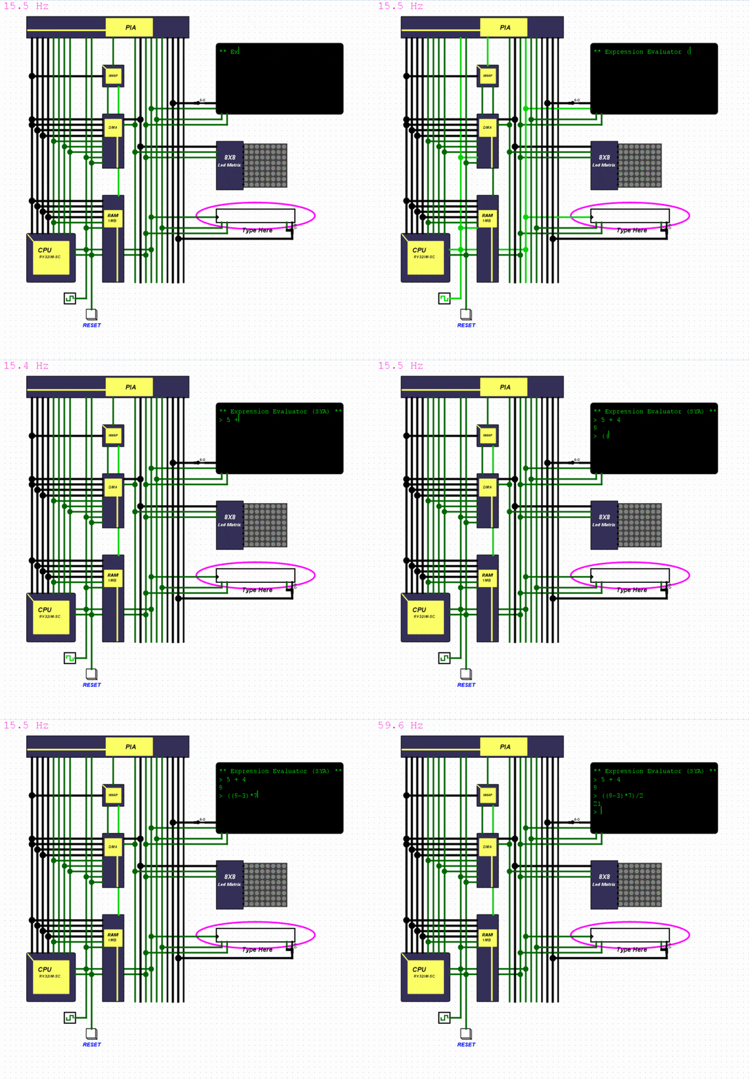
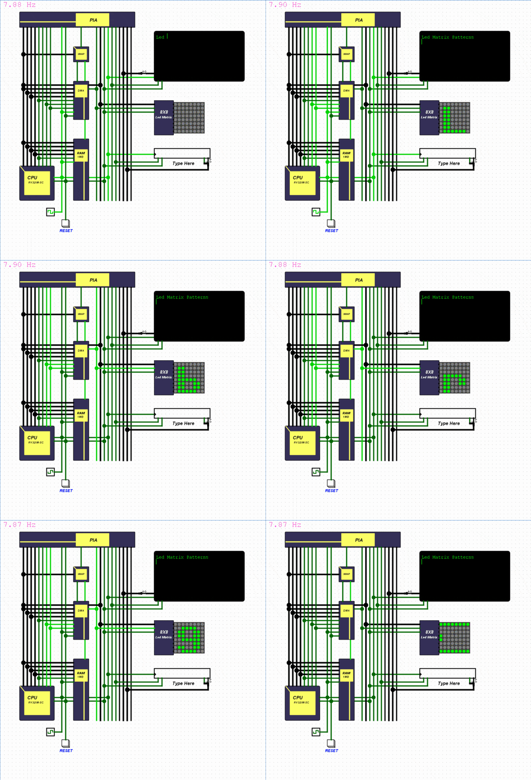
An enhanced yet simplified version of the original RISC-V-Computer.
1. Redesigned CPU with two versions to choose from
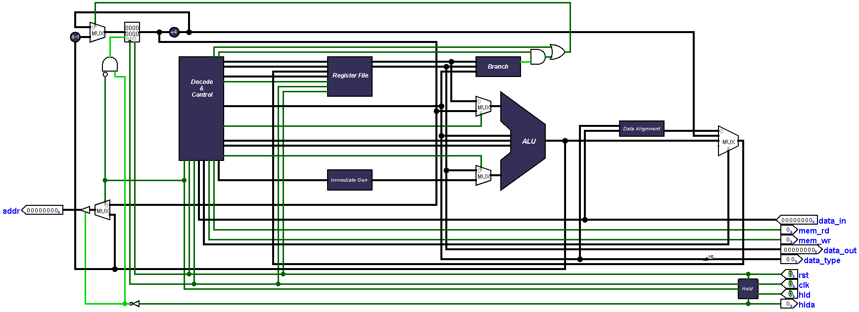
   Single-Cycle
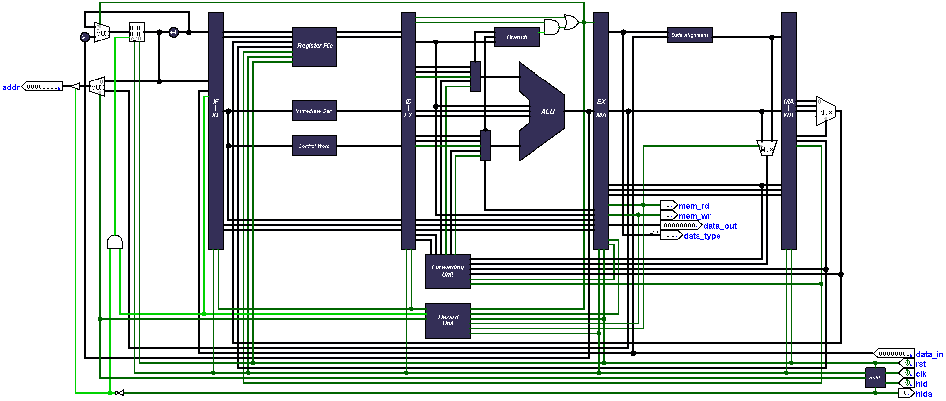
   5-Stage-Pipelined
2. Simplified Main Memory module
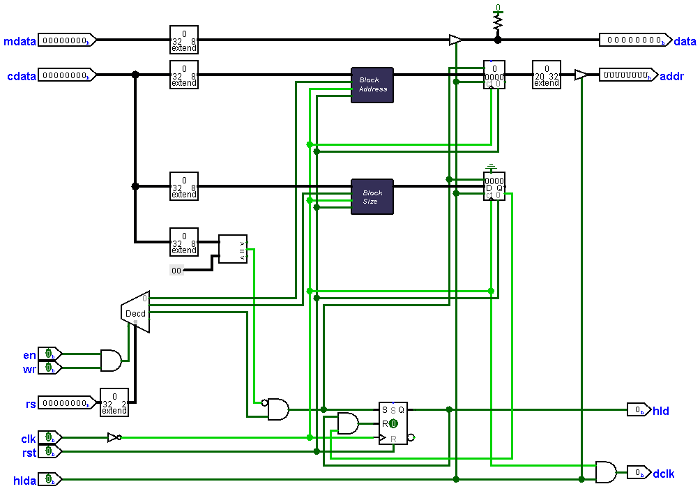
3. DMA (Direct Memory Access)
4. Redesigned I/O Interface
- Motivation
- CPU
- Memory
- DMA (Direct Memory Access)
- PIA (Peripheral Interface Adapter)
- Memory map
- Loading a program
- Demo
The original RISC-V Computer was intended to be a practical approach for understanding computer
organization and architecture with the help of RISC-V ISA, however the design was overly
complicated and hard to understand in fact understanding how the CPU works will
require hours of reverse engineering work, worse yet, the main memory module was unnecessarily
large being 128MB in size divide as 8(eight) 16MB sized banks and worst of all, no design documentation.

I have made several attempts to simplify the original design but all ended up failing, mainly due to the way
the original CPU was designed and implemented "RTL style" so a complete redesign was the only way to go.
Completely redesigned, the new simplified design has a smaller footprint-
based on Von Neumann architecture, and both CPUs implements the RV32IM extensions.
it also features hold-hold acknowledge mechanism for DMA support
When the hld pin is asserted the CPU sets the hlda signal if it's not currently executing
any memory related instruction.

The pipelined version implements the classical 5-Stage RISC pipeline [IF, ID, EX, MA, WB] and supports
hazard detection and operand forwarding.
One case where forwarding cannot help eliminate hazards is when an instruction
tries to read a register following a load instruction that writes the same register.
The data is still being read from memory in clock cycle 4 while the ALU is performing
the operation for the following instruction. hence we must stall the pipeline for the
combination of load followed by an instruction that reads its result.

But this is not considered an issue in our design, since all memory instructions
already stall the CPU for one clock cycle due to single memory design. So no need to
add any more logic to the Hazard unit regarding that case.
The simplified main memory module has been downgraded to 20-bit address space providing
1MB access for both code and data.
The block transfer memory-to-io DMA is the killer new feature! providing blazing fast
data transfer with speeds up to 280 bytes/s (speed is host machine dependent) and can transfer up to 64KB
worth of data.

How to use
	The DMA contains three main registers
		1. Block address (20-bit)
		2. Block size (16-bit)
		3. Start transfer (strobe)

	In order to set the address register correctly the 20-bit block address must be
	written to DMA as three successive byte writes this also implies to the 16-bit
	-block address register where two successive byte write must be made.

	To start data transfer any arbitrary non zero value must be written to transfer strobe register.
	the DMA halts the CPU until data transfer is completed.
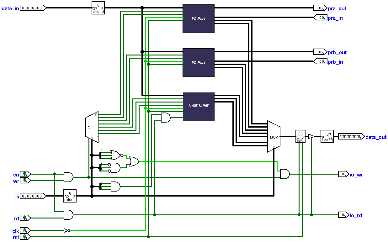
Inspired by the 6522 PIA the new I/O interface provides a more flexible way for interfacing
I/O devices. featuring

	1. Two per bit programmable 8-bit I/O ports (PRA, PRB) where each bit can be configured
	  as Input or Output individually by writing the data direction registers (DDRA, DDRB),
	  writing a value to DDR sets the corresponding bit as either read only or write only
		"1" Write only
		"0" Read only

	2. A programmable 8-bit timer with clock prescaler (divide by 1,2,3,4) and two operation modes
		 1. Continuous-mode
		 2. Compare-mode

		How to use
		    The timer contains four registers
			1. Timer count (8-bit) holds current timer value
			2. Timer compare (8-bit) used for comparison in compare mode
			3. Timer control (8-bit) used to configure the timer
			4. Timer Flag (8-bit) indicates timer overflow

		    Timer control register
			[-][-][-][-][PS1][PS0][MOD][ST]

		   ST: Timer Start/Stop (bit 0)
			"0" stop
			"1" start

		   MOD: Timer mode (bit1)
			"0" continuous
			"1" compare

		   PS1-PS0: Timer prescaler
			"00" divide clock by 1
			"01" divide clock by 2
			"10" divide clock by 3
			"11" divide clock by 4

		Continuous-mode
			In this mode the timer increments until it overflows setting the Timer flag register to (0xFF)
			then it wraps around to zero.
			The timer can be loaded with any offset value at any time by writing to Timer count register.

		Compare-mode
			In this mode the count register value is compared with the compare register, if they match
			the Timer flag is set to (0xFF) and the timer count register is reset to back zero.


		In both modes the timer continues to increment until it stopped manually be the programmer.
		The flag register is clear by reading the register value.
PIA
	0xFFFF7		TIMER_FLAG    (R)
	0xFFFF6		TIMER_CONTROL (R/W)
	0xFFFF5		TIMER_COMPARE (W)
	0xFFFF4		TIMER_COUNT   (R/W)
	0xFFFF3		DDRB	      (R/W)
	0xFFFF2		PRB	      (R/W)
	0xFFFF1		DDRA	      (R/W)
	0xFFFF0		PRA	      (R/W)

DMA
	0xFFFF8		BLOCK_ADDRESS         (W)
	0xFFFF9		BLOCK_SIZE    	      (W)
	0xFFFFA		START_TRANSFER_STROBE (W)

Main Memory
	0xFFEFF-0x00000 (can be configured by linker file)

(R/W) Read and write
(R)   Read only
(W)   Write only
Tested in Logisim-evolution v3.7.2
