This section explores various 32-bit signed adders implemented in Verilog. The focus is on studying the characteristics of different adder implementations and evaluating their performance. A comprehensive testbench validates each adder, and synthesis is performed with specified constraints.
This part covers the following adders:
- Verilog (+) version of adders
- Ripple Carry Adder
- Carry Look-Ahead Adder
- Carry Bypass Adder
- Carry Select Adder
Test Cases Covered:
- Overflow of positive numbers.
- Overflow of negative numbers.
- Addition of positive and negative numbers.
- Addition of positive and positive numbers.
- Addition of negative and negative numbers.
- Additional 3 random test cases.
In this section, 32-bit signed multipliers are designed and implemented in Verilog. The chosen adder from Part 1 is integrated into the multiplier implementations. A comprehensive testbench is created, and synthesis is performed with specified constraints.
This part covers the following multipliers:
- Verilog (*) version of multiplier
- Multiplier Tree (combinational)
- Sequential Multiplier using shift & accumulate
- Booth Algorithm (Original algorithm)
Test Cases Covered:
- Multiplication of positive and negative numbers.
- Multiplication of positive and positive numbers.
- Multiplication of negative and negative numbers.
- Multiplication of negative and positive numbers.
- Multiplication by zero.
- Multiplication by 1.
- Additional 2 random test cases.
then the most appropriate multiplier was chosen to create a floating-point multiplier (IEEE-standard).
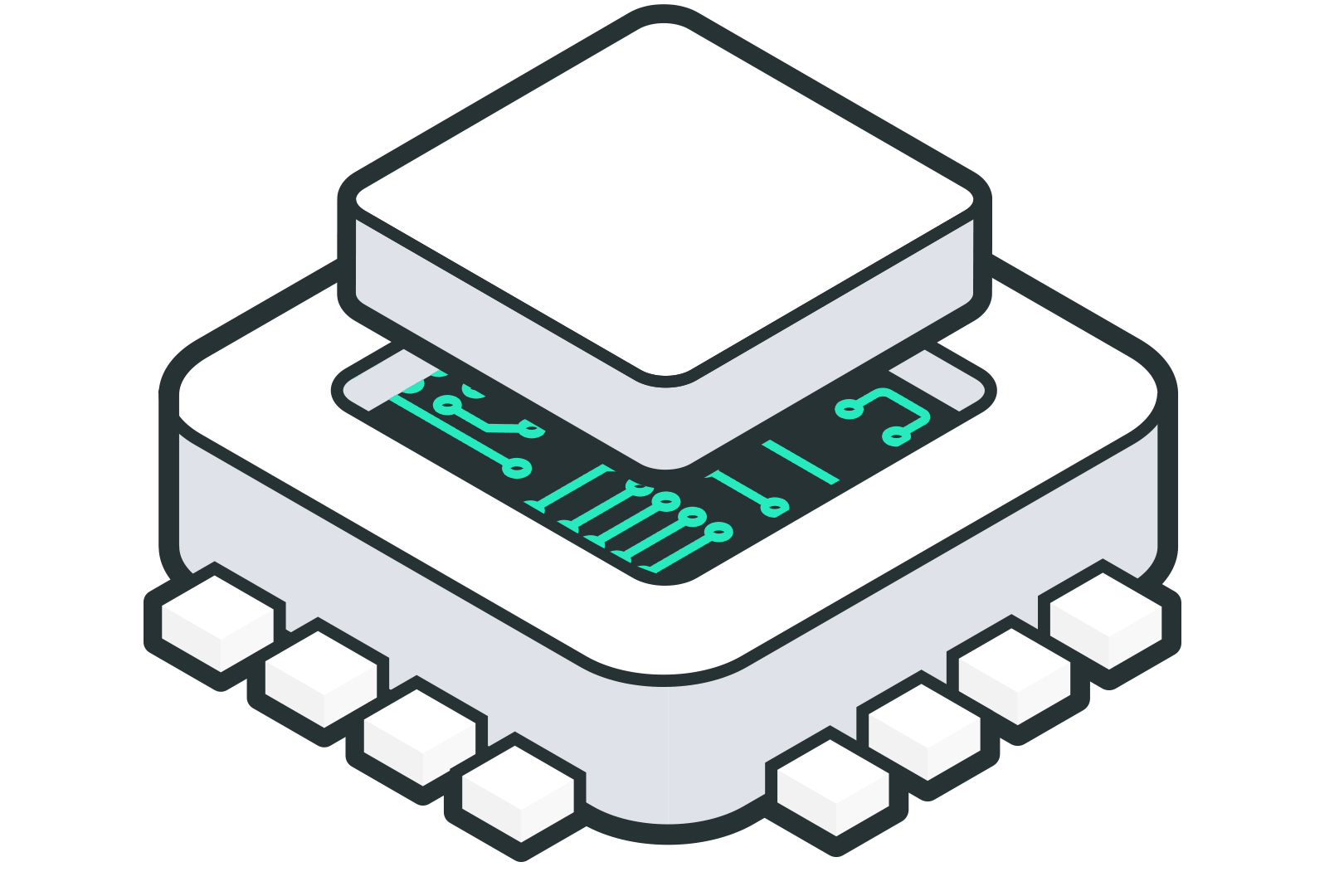
This section involves the integration of the Phase One adder and Phase Two multiplier to generate a chip. Synthesis, placement, and routing are performed with specified constraints. Post-routing simulation is conducted, and GDS files are generated for each design.
This part summarizes the synthesis, placement, routing, post-routing simulation, and GDS file generation processes for the final chip.

Menna |

Eman |

Nesma |

Sara |