
A lightweight CPU core for basic RV32I instructions running on Minisys. Project for CS214 Computer Organization.
For Chinese README, see README_CN.
| SID | Name | Contribution Rate |
|---|---|---|
| 12111624 | GuTaoZi | 50% |
| 12112012 | Jayfeather233 | 50% |
| Struct | ISA | Doc | IF | ID | EX | MEM | WB | IO | ASM | Sim | Video | |
|---|---|---|---|---|---|---|---|---|---|---|---|---|
| 🍑 | ✔ | ✔ | ✔ | ✔ | ✔ | ✔ | ✔ | ✔ | ||||
| 🪶 | ✔ | ✔ | ✔ | ✔ | ✔ | ✔ | ✔ | ✔ | ✔ |
* Uncountable detailed contributions are omitted here.
This project is written in Verilog Coding Style.
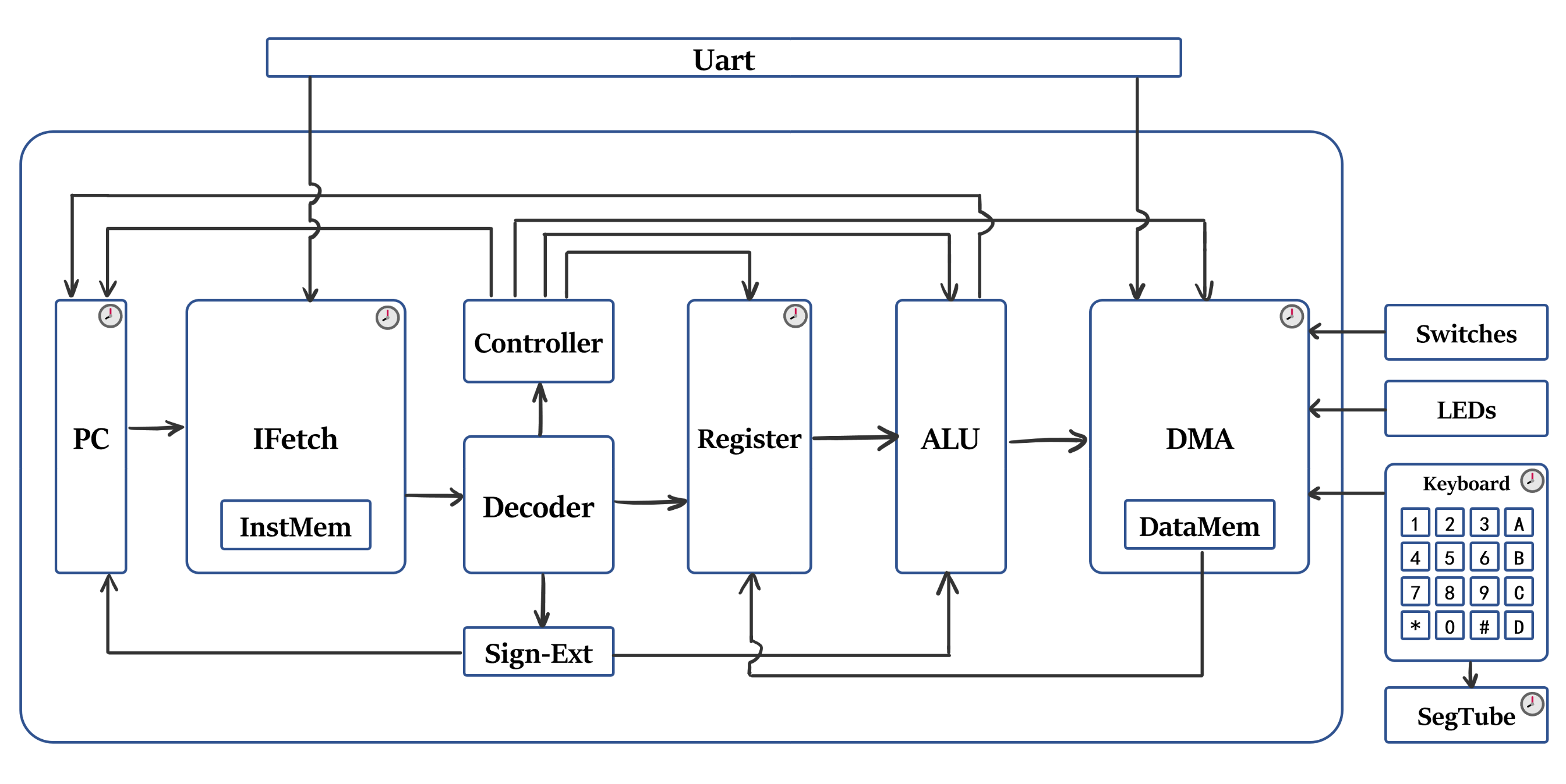
Harvard architecture
CPU frequency: 25 MHz
CPI: 2 cycles/instruction
32-bit Registers: x0 - x31
This custom ISA is designed based on RV32I.
32-bit Instructions, 32 General Registers of 32-bit width.
Some signed instructions beyond RV32I are implemented in this ISA.
For more details, see Feather ISA.
- FPGA frequency: 100 MHz
- CPU frequency: 25 MHz
- Uart interface, for instruction and data memory input
- 4X4 matrix keyboard, for memory-mapped input
- 24 switches, for debugging input
- Reset button: P5
- Input acknowledge button: P10
- Input reset button: P1
- Debugging state button: R1
- 8 segment tubes, displaying input data and CPU state information
- 24 leds, for memory-mapped output
| Port | I/O | Src/Dst | Description |
| fpga_clk | I | Hardware | FPGA clock signal |
| rst_raw | I | Hardware | Reset signal before de-jittered |
| upg_rx | I | Uart | Uart input data |
| kb_row | I | Hardware | Keyboard row signal |
| debug_btn | I | Hardware | Debug button signal |
| sw | I | Hardware | Switches signal |
| kb_ack_btn | I | Hardware | Keyboard ACK signal |
| kb_cancel_btn | I | Hardware | Keyboard input reset signal |
| filter_test_btn | I | Hardware | Filter test button signal |
| kb_col | O | Hardware | Keyboard col signal |
| upg_tx | O | Uart | Uart send back data |
| led_o | O | Hardware | LED state |
| seg_cho | O | Hardware | Segment tube select signal |
| seg_lit | O | Hardware | Segment tube data to display |
| Port | I/O | Src/Dst | Description |
| i_clk | I | Top | CPU clock signal |
| i_rst | I | Hardware | Reset signal |
| i_Jal | I | InstDecoder | Jal instruction enable |
| i_Jalr | I | InstDecoder | Jalr instruction enable |
| i_pc_en | I | Top | PC update enable |
| i_branch | I | InstDecoder | Branch instruction enable |
| i_Jal_imm | I | InstDecoder | Jal immediate |
| i_alu_val | I | InstDecoder | Result of ALU for updating PC |
| o_pc | O | Top | Current PC |
| o_next_pc | O | Top | Next PC, for debugging |
| o_pc_rb | O | Top | PC to write back for Jal(r) |
| Port | I/O | Src/Dst | Description |
| i_pc | I | PC | Program counter |
| i_clk | I | Hardware | FPGA clock signal |
| i_uart_ena | I | Uart | Uart-write enable signal |
| i_uart_done | I | Uart | Uart write-complete signal |
| i_uart_clk | I | Uart | Uart clock signal |
| i_uart_addr | I | Uart | Uart-write memory address |
| i_uart_data | I | Uart | Data to write in, from uart |
| o_inst | O | ID | Instruction read out |
| Port | I/O | Src/Dst | Description |
| i_inst | I | InstMem | Instruction to decode |
| o_rs1_idx | O | ALU | Index of first register |
| o_rs2_idx | O | ALU | Index of second register |
| o_imm | O | ALU | Immediate number decoded |
| o_alu_op | O | ALU | ALU operator number |
| o_mem_read | O | DMA | Memory read enable |
| o_mem_write | O | DMA | Memory write enable |
| o_mem_to_reg | O | DMA | Memory write back |
| o_inst_type | O | ALU | Instruction type |
| funct10 | O | Top | {funct3, funct7} |
| Port | I/O | Src/Dst | Description |
| i_read_addr1 | I | InstDecoder | Index of first register |
| i_read_addr2 | I | InstDecoder | Index of second register |
| i_write_addr | I | InstDecoder | Index of write-back register |
| i_write_data | I | Top | Data to write back |
| i_write_en | I | Top | Write back enable |
| i_clk | I | Top | CPU clock signal |
| i_rst | I | Hardware | Reset signal |
| i_debug_idx | I | Top | Index of register to display |
| o_read_data1 | O | ALU | Value of first register |
| o_read_data2 | O | ALU | Value of second register |
| o_debug_data | O | ALU | Value of display register |
| Port | I/O | Src/Dst | Description |
| i_src1 | I | InstDecoder | First operand |
| i_src2 | I | InstDecoder | Second operand |
| i_branch_val_i | I | InstDecoder | Immediate for B inst |
| i_ALU_op | I | InstDecoder | ALU operator number |
| i_rst | I | Top | Reset signal |
| o_ALU_ouput | O | Top | Result |
| o_overflow | O | Top | Overflow identifier |
| Port | I/O | Src/Dst | Description |
| hdw_clk | I | Top | FPGA clock signal |
| cpu_clk | I | Top | CPU clock signal |
| cpu_mem_ena | I | Top | CPU-access memory signal |
| cpu_addr | I | Top | CPU-access memory address |
| cpu_write_data | I | Top | Data to write in, from CPU |
| cpu_mem_read_ena | I | Top | CPU-read memory signal |
| cpu_mem_write_ena | I | Top | CPU-write memory signal |
| hdw_sw_data | I | Hardware | MMIO data from switches |
| hdw_keybd_data | I | Hardware | MMIO data from keyboard |
| hdw_ack_btn | I | Hardware | MMIO data from ACK button |
| uart_ena | I | Uart | Uart-write memory signal |
| uart_done | I | Uart | Uart-complete signal |
| uart_clk | I | Uart | Uart clock signal |
| uart_addr | I | Uart | Uart-write memory address |
| uart_data | I | Uart | Data to write in, from uart |
| read_data | O | Top | Data read from data memory |
| hdw_led_data | O | Hardware | MMIO data for leds |
| Port | I/O | Src/Dst | Description |
| i_addr | I | DMA | The address of demanded data |
| i_write_data | I | DMA | The data to write in |
| i_mem_read | I | DMA | Read enable |
| i_mem_write | I | DMA | Write enable |
| i_clk | I | Hardware | FPGA clock signal |
| o_read_data | O | DMA | Data read out |
| Method | Module | Result | Descriptions |
|---|---|---|---|
| Simulation | InstDecoder | ✔ | Check whether the combinational logic module correctly decodes the instructions |
| Simulation | Filter | ✔ | The filter de-jitters the input signals and outputs stable signals. |
| On-board | Uart | ✔ | The uart interface works well. |
| On-board | DMA and IO interfaces | ✔ | The keyboard, segtubes, switches and LEDs work, and DMA accesses the memory correctly. |
| On-board | PC | ✔ | PC is updated correctly according to controller and ALU. |
| On-board | ALU | ✔ | ALU correctly calculates the results for all instructions. |
| On-board | Register | ✔ | The input and output of registers are correct. |
| Method | Object | Result | Descriptions |
|---|---|---|---|
| Simulation | ID - EX - Reg | ✔ | The combinatorial part works. |
| On-board | Top | ✔ | The usability test of all types of instructions |
| On-board | Top | ✔ | Test scenario 1. See project requirement |
| On-board | Top | ✔ | Test scenario 2. See project requirement |
| Testcase | Descriptions | Result |
|---|---|---|
| Marquee | Use MMIO to control the running speed of the marquee. | ✔ |
| Fibonacci | Calculate the Fibonacci sequence with fast matrix exponential. | ✔ |
In this project, we implement a single-cycle CPU for FeatherISA running on Minisys from scratch without referencing others' implementations. Though many bugs were met during the process of development, they were then solved with great efforts. This is really meaningful for understanding the architectures of computers, and stimulates our interest of hardware-software cooperating development.
Great thanks for Prof. Zhang, TA Wang Wei, SAs, and everyone else who contributes to the development of this project!
- Different ISAs bring about different architectures
- Writing bitstreams to the board always fails for the first time for unknown reason, kind of annoying
- The hold time violation leads to some sequential time failure
- VIVADO cooperates BAD with Git
- Simulation on modules
- Implement debug modes, output the current information of CPU
See CHANGELOG.md.
- CPU Features
- ISA Design
- Address Space Design
- Fast Single Cycle Design
- Debugging
- CPU Interfaces
- Clock
- Reset
- Uart
- Others: Keyboard, segment tubes
- Internal Structures
- Module interconnections
- Module introduction
- Tests
- Basic testcases #1
- Basic testcases #2
- Bonus testcases
- Video for bonus part
- Summary