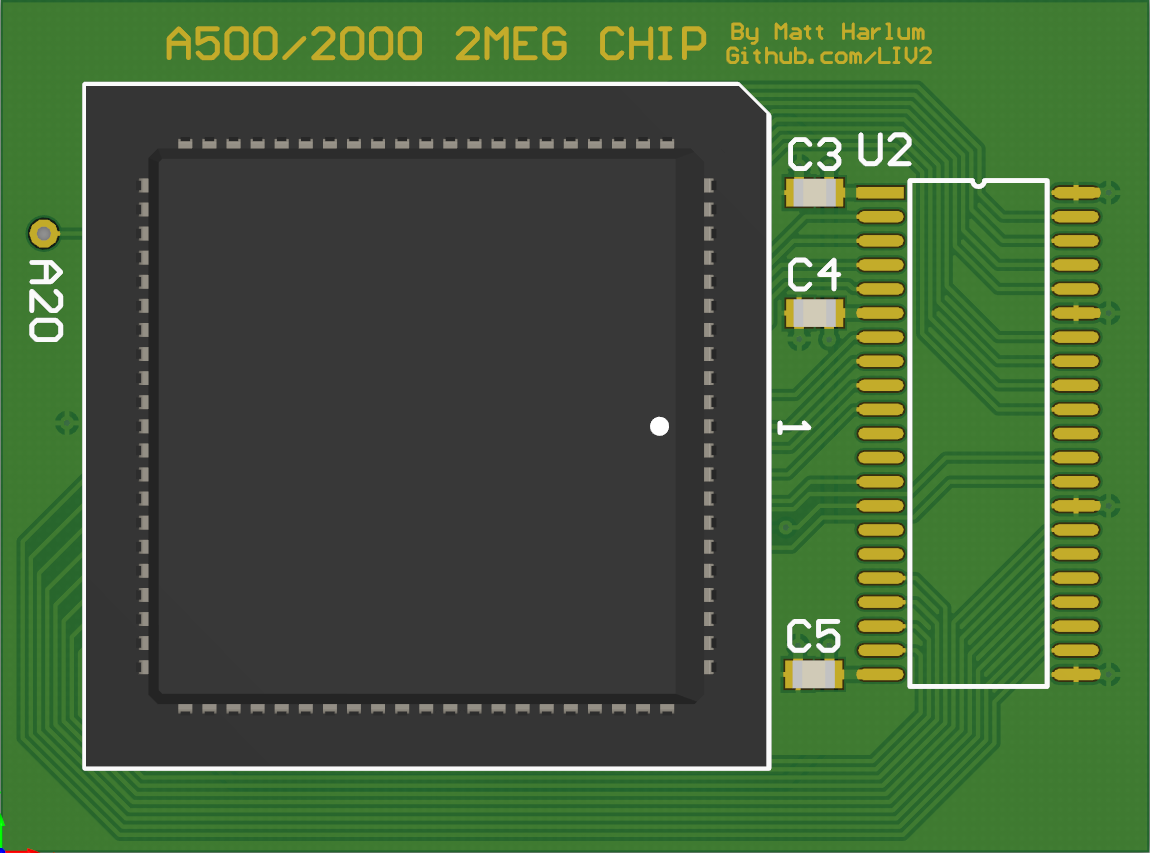
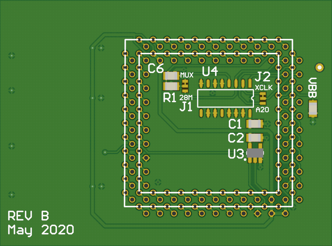
This is an adapter board to retrofit a 2MB Agnus into an Amiga 500/2000 and also includes 2MB of chip ram
A version that uses a PLCC plug instead of pinheaders is available Here
- Solder the DRAM, U4, U3
- Solder the Capacitors & Resistor (Only fit VBB capacitor if your Agnus says VBB on the top!)
- Solder the PLCC Socket making sure that the socket aligns exactly with the outline on the top of the PCB!
- After soldering the socket, you may want to trim the joints down to the PCB to make soldering the pin headers easier.
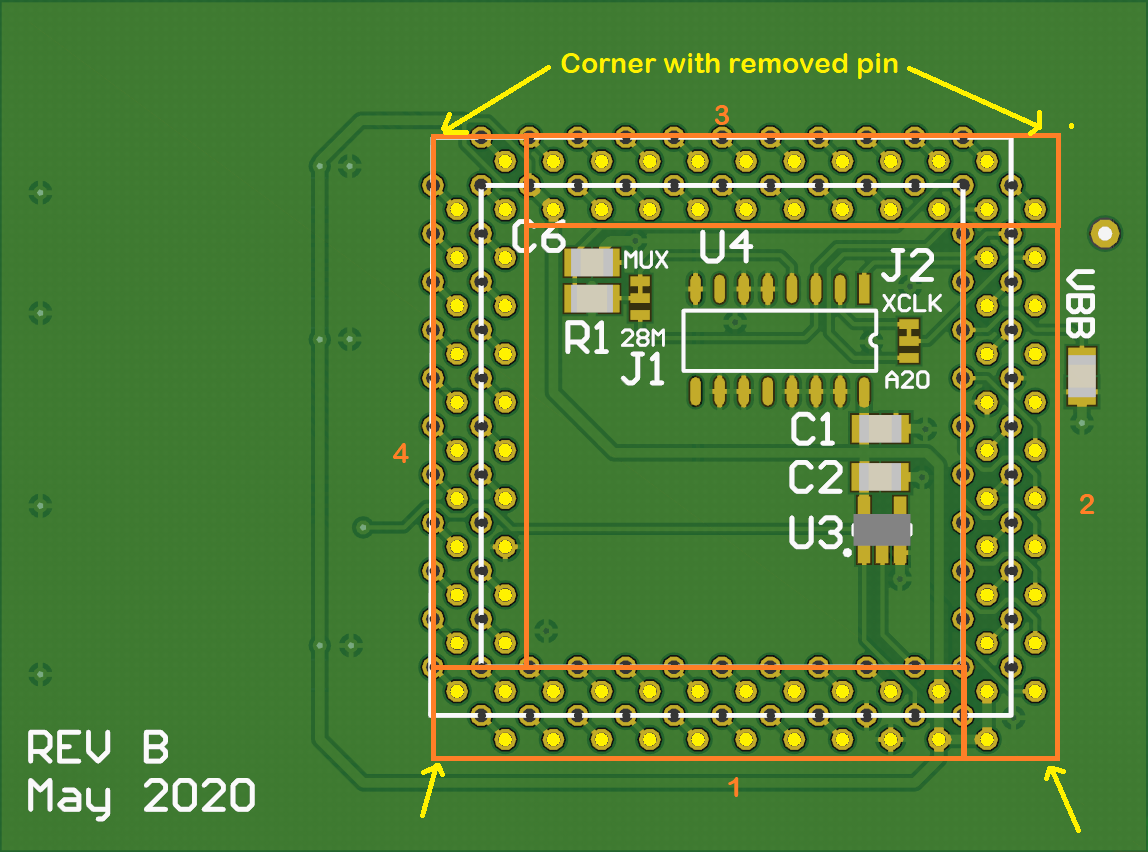
Be careful when trimming the leads that you don't scratch the PCB solder mask! - Prepare the pin headers by removing a pin from this corner of each as indicated here:
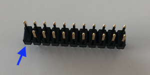
- Insert one of the pin headers just far enough for it to hold, making sure that it is level.
The side with the removed pin goes where indicated by the yellow arrow
I recommend doing them one by one in the order indicated:
If you will be soldering to the Amiga rather than using sockets, I would recommend soldering the long side of the pins to the adapter
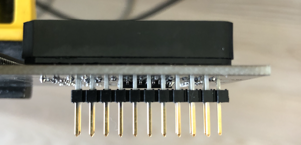
- Solder in each pin, don't use too much solder!
- Repeat for each pin header
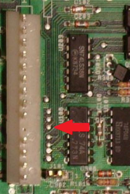
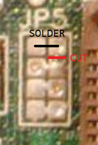
- Solder a wire to A20 and connect the other end at one of the following locations:
- Gary pin 36
- CPU pin 48
- JP5 Top left pad (A500 Rev 6)
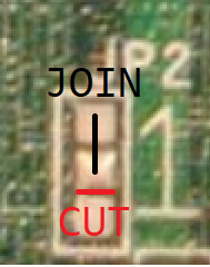
- Make sure that JP2 is set as shown:
- Carefully desolder & remove the Agnus socket
- Remove the same corner pin from each pin socket and solder them in replacing the agnus socket
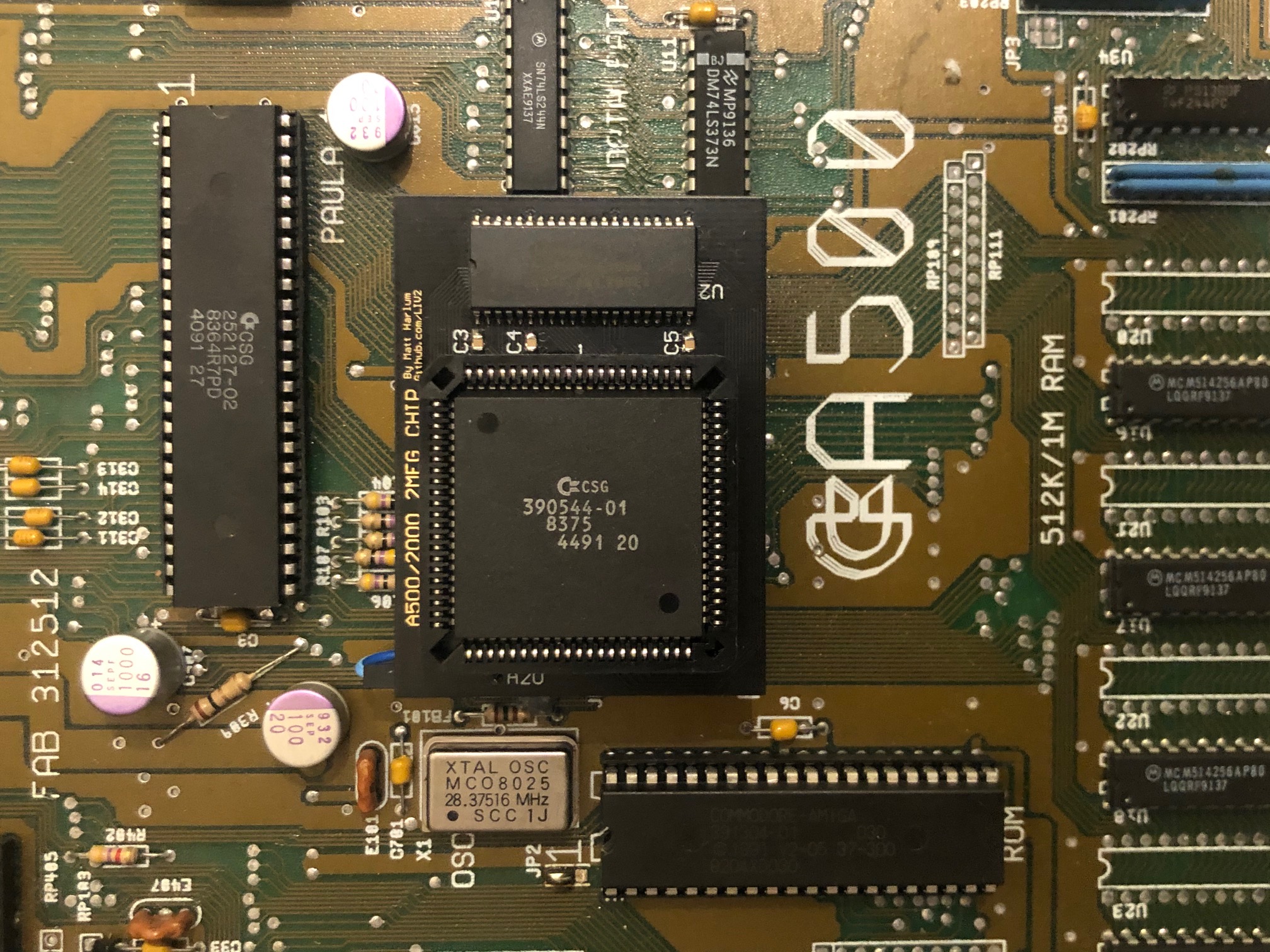
- Insert the adapter
To make sure it is installed the correct way, pay attention to the marking of "1" on the PCB and on the Amiga they must match
On a Rev 6A Amiga 500 this means that the ram will be on the right hand side, on a Rev 5 it will be pointing downwards instead.
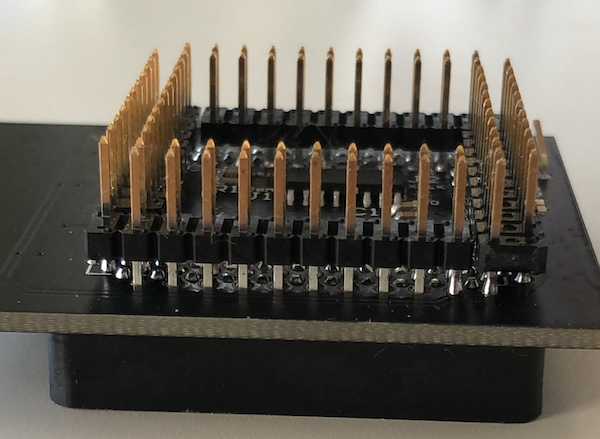
look from the sides to make sure the pins are going in to the headers
Solder a wire to A20 and connect the other end at one of the following locations:
- Gary pin 36
- CPU pin 48
- JP5 Top left pad (A500 Rev 6)
Solder a wire to A20 and connect the other end at one of the following locations:
A20 is available from Pin 15 of U28 on the Rejuvinator
The default jumper settings do not need to be changed and will work on all systems.
Rev 6A Amiga 500's have jumpers that can be used to provide the A20 signal on pin 35 instead of XCLK This allows us to use this adapter without having to add the wire to A20 but note this will mean you cannot use a genlock on this Amiga!
In this case you must set J1 to 28M to bypass the XCLK/28M Mux then set J2 of the adapter to A20
If you wish to do this then you will also need to change the jumper settings at J5 on your A500 motherboard
| Component | Location | QTY | Link | Notes |
|---|---|---|---|---|
| Ceramic Capacitor, 0.1uF, 0805 | C1-5,C7 | 6 | Mouser | |
| Ceramic Capacitor, 22pF, 0805 | C6 | 1 | Mouser | |
| Resistor, 150 Ohm, 0805 | R1 | 1 | Mouser | |
| 74AHC1G08 Single 2-Input AND Gate, SOT-23-5 | U3 | 1 | Mouser | |
| 74AHCT158 Quad 2-input Multiplexer, SOIC-16 | U4 | 1 | Mouser | Optional, set J1 to "28M" to bypass |
| PLCC-84 Socket, Through-hole | U1 | 1 | Mouser | |
| 5V, 1Mx16 EDO/FPM DRAM, SOJ-42 - K4F151611 - K4E151611 - GM71C18163C - AS4C1M16E5 |
U2 | 1 | eBay, Aliexpress etc | |
| 22-Pin, 2 Row Female header | 4 | Mouser | ||
| 22-Pin, 2 Row Male header | 4 | Mouser |
