基于AXI接口的高速SD卡控制器
该项目中的sdcmd_ctrl.sv与sd_reader.sv文件中的代码部分参考了https://github.com/WangXuan95/FPGA-SDcard-Reader项目,
同时也参考了SD Specifications Part 1 Physical Layer Speicifcation Version 3.00 April 16, 2009手册。
该SD卡控制器拥有如下特性:
- 运行在50MHz SDIO 4-wire 高速模式下
- 工作在SD卡多块传输模型
- 传输速率最高可达23MB/s
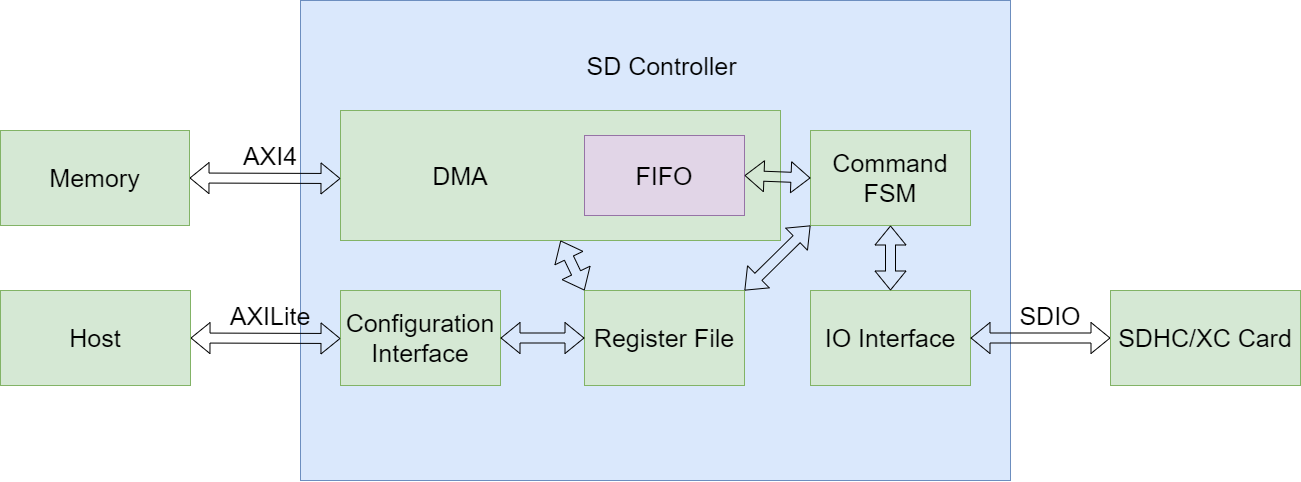
- AXI4接口的主动DMA(支持256突发)
- AXILite配置接口
- 一次传输最大支持4GiB的数据
- 起始扇区最大可为0xFFFFFFFF,即可以访问SD卡前1TiB整个范围的任意数据
- 仅支持数据只读
代码位于rtl目录下,各个文件的用途如下所示:
| 文件名 | 描述 |
|---|---|
| sdcmd_ctrl.sv | SDIO PHY层,实现了基本的SDIO时序 |
| sd_reader.sv | SDIO MAC层,实现了SD卡的基础命令集和扇区读取控制 |
| sd_controller_regfile.sv | 控制器的AXILite寄存器配置接口实现及配置寄存器实现 |
| sd_controller_ping_pong_buffer.sv | Ping/Pong Buffer |
| sd_controller_axi_writer.sv | 支持只写256突发的AXI4 DMA |
| sd_controller.sv | SD卡控制器顶层 |
| sd_controller_wrapper.v | SD卡控制器的Verilog包装层 |
该控制器启动时首先输出400KHz时钟,在完成SD卡基础配置流程后输出25MHz时钟,在切换到高速模式后输出50MHz时钟。
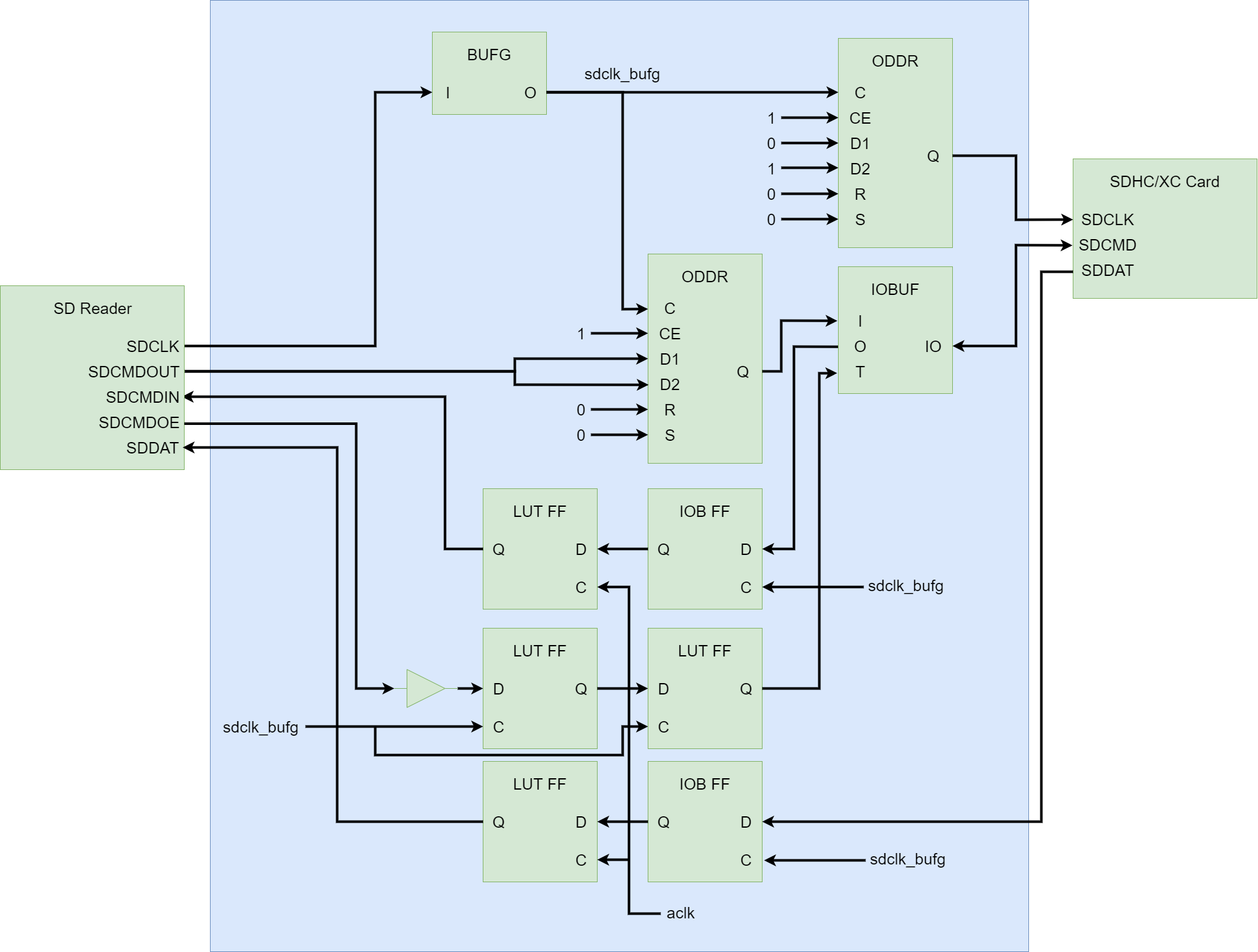
为了实现如此高速的传输,该控制器的实现使用了一些Xilinx FPGA原语及约束,其中原语部分在Verilog包装层中实现,原理图如下:
其中:
- BUFG用于将SD Reader输出的时钟变换到FPGA专用时钟网络中以便改善各个FF的Timing
- ODDR用于将时钟与命令对齐输出,其中最上面的ODDR用于输出时钟,并且由于将D1接为0,D2接为1,ODDR将会输出一个与原时钟相位差180度的时钟,由于SDCMDOUT在SDCLK改变,在输出时钟反相后,SDCMD相对于输出时钟的Setup/Hold Timing都可以得到很大的改善,以便为信号在PCB上的走线提供足够的裕量。
- 将SDCMDOE打两拍是为了和输出的SDCMDOUT信号对齐,保证三态门在正确的时机切换。
- SDCMDIN先在IOB的FF上打一拍(此时信号属于sdclk_bufg时钟域),这同样保证信号经过PCB走线之后仍然拥有足够的Timing裕量。接下来将IOB FF输出的信号在LUT FF上再打一拍,此时采用的时钟是aclk,也就是控制器时钟(本例为100MHz),实现跨时钟域。这里之所以采用这种方式跨时钟域,是因为sdclk_bufg本身就是aclk的生成时钟,因此综合器STA可以正确计算Setup/Hold Time,使得一般情况下跨时钟域的亚稳态问题不会在这种情况下出现。
- SDDAT也是类似的情形,先在IOB FF上通过sdclk_bufg打一拍,然后用aclk打一拍,送入SDIO Reader。
顶层模块为sd_controller_wrapper,其中各端口描述如下:
| 端口名 | 方向 | 描述 |
|---|---|---|
| aclk | I | 控制器时钟(也是AXI4和AXILite时钟),必须为100MHz |
| aresetn | I | 控制器复位信号(也是AXI4和AXILite总线复位信号),低有效 |
| axilite_* | I/O | AXILite Slave配置接口信号(配置空间大小4KB,地址数据宽度均为32bit) |
| axi_* | I/O | AXI4 Master DMA Write-Only接口信号(地址数据宽度均为32bit) |
| sdclk | O | SD卡时钟线 |
| sdcmd | I/O | SD卡命令线 |
| sddat | I | SD卡数据线 |
| card_type | O | SD卡类型信号 |
| card_stat | O | SD卡控制器状态机当前状态 |
| interrupt | O | 中断信号,高有效 |
| test_* | O | 仅供测试使用 |
为了让综合器正确计算跨时钟域的STA,需要加入如下生成时钟约束(控制器时钟100MHz,SDIO时钟最大50MHz,按照2分频设置):
create_generated_clock -name sdclk -source [get_pins top_design_i/clk_wiz_main/clk_out3] -divide_by 2 [get_pins top_design_i/sd_controller_wrapper_0/inst/sd_controller_inst/sd_reader_inst/sdcmd_ctrl_inst/sdclk_reg/Q]
其中注意将top_design_i/clk_wiz_main/clk_out3改为正确的控制器时钟。
目前已在KC705平台上测试通过,FPGA为XC7K325T-2FFG900,如需要使用其它的FPGA,注意替换sd_controller_wrapper.v中的原语。
该模块可以直接被Verilog或SystemVerilog引用,也可以直接加入Vivado的Block Design中使用。
在src目录中附带了示例的软件驱动可供使用,该驱动提供了如下函数:
| 函数 | 描述 |
|---|---|
| sdcard_reset | 复位SD卡控制器 |
| wait_sdcard_ready | 等待SD卡控制器就绪(有超时检测,超时会自动重发命令) |
| sdcard_read | 读取SD卡数据,该函数会等待SD卡控制器就绪后再发起命令(有超时检测,超时会自动重发命令) |
| sdcard_is_busy | 返回TRUE表示SD卡控制器繁忙 |
| sdcard_get_progress | 获取SD卡控制器进度 |
其中,为了超时功能能够支持运行,需要用户填充sdcard.c中的get_ms_time函数,该函数的作用是范围以毫秒为单位的系统时间。
同时注意修改sdc变量中的地址,指向正确的SD卡控制器基地址。
| 偏移 | 名称 | 属性 | 描述 |
|---|---|---|---|
| 0x00 | CTRL | RW | 控制寄存器 |
| 0x04 | STAT | RO(INT位为RW) | 状态寄存器 |
| 0x08 | DSTADDR | RW | 目标地址 |
| 0x0C | STARTSECTOR | RW | 起始扇区 |
| 0x10 | SECTORNUM | RW | 扇区数(512字节为单位,必须为偶数) |
| 0x14 | PROGRESS | RO | 当前进度(字节数) |
| 0x18 | RESET | RW | 复位寄存器 |
RW - 读写 RO - 只读
控制寄存器:
| 位 | 名称 | 描述 |
|---|---|---|
| 31:2 | 保留 | 读恒为0 |
| 1 | INT_EN | 中断使能(1为使能,0为失能) |
| 0 | START | 启动传输(该位写1启动,读恒为0) |
状态寄存器:
| 位 | 名称 | 描述 |
|---|---|---|
| 31:9 | 保留 | 读恒为0 |
| 8:5 | Card Stat | SD卡控制器状态机 |
| 4:3 | Card Type | SD卡类型 |
| 2 | INT | 中断挂起(该位写1清除中断) |
| 1 | DMA Error | DMA写Memory发送错误 |
| 0 | BUSY | 正在传输中(为1表示正在传输中,为0表示空闲) |
Card Stat的取值及含义如下:
| 取值 | 含义 |
|---|---|
| 0000 | 正在发送CMD0(GO_IDLE_STATE)命令,控制器保持空闲状态 |
| 0001 | 正在发送CMD8(SEND_IF_COND)命令并等待响应 |
| 0010 | 正在发送CMD55(APP_CMD)命令并等待响应 |
| 0011 | 正在发送ACMD41(SD_SEND_OP_COND)命令并等待响应 |
| 0100 | 正在发送CMD2(ALL_SEND_CID)命令并等待响应 |
| 0101 | 正在发送CMD3(SEND_RELATIVE_ADDR)命令并等待响应 |
| 0110 | 正在发送CMD7(SELECT_CARD)命令并等待响应 |
| 0111 | 正在发送CMD55(APP_CMD)命令并等待响应 |
| 1000 | 正在发送ACMD6(SET_BUS_WIDTH)命令并等待响应 |
| 1001 | 正在发送CMD6(SWITCH_FUNC)命令并等待响应 |
| 1010 | 正在发送CMD16(SET_BLOCKLEN)命令并等待响应 |
| 1011 | 准备发送CMD18(READ_MULTIPLE_BLOCK)命令 |
| 1100 | 正在等待CMD18(READ_MULTIPLE_BLOCK)命令响应 |
| 1101 | 正在从SD卡接收数据 |
| 1110 | 正在发送CMD12(STOP_TRANSMISSION)命令并等待响应 |
| 1111 | 等待数据接收状态机到达读取结束状态 |
Card Type的取值及含义如下:
| 取值 | 含义 |
|---|---|
| 0000 | 未知类型 |
| 0001 | SD 1.0卡 |
| 0010 | SD 2.0卡 |
| 0011 | SDHC/XC 2.0卡 |
| 0100 | 或许是SD 1.0卡(只作为中间态,不作为最终态) |
| 0101~1111 | 保留 |
目的地址寄存器:
| 位 | 名称 | 描述 |
|---|---|---|
| 31:0 | DSTADDR | 目标地址 |
起始扇区寄存器:
| 位 | 名称 | 描述 |
|---|---|---|
| 31:0 | STARTSECTOR | 起始扇区(一个扇区为512字节,不要超过SD卡容量范围) |
扇区数量寄存器:
| 位 | 名称 | 描述 |
|---|---|---|
| 31:23 | 保留 | 读恒为0 |
| 22:1 | SECTORNUM | 扇区数(因为一次传输1KB数据,因此要求扇区数必须为偶数且不能为0,这也是AXI突发为256的原因,256 * 32bit = 1KiB) |
| 0 | 保留 | 读恒为0 |
当前进度寄存器:
| 位 | 名称 | 描述 |
|---|---|---|
| 31:0 | PROGRESS | 当前DMA已传输完成数据量(字节数) |
复位寄存器:
| 位 | 名称 | 描述 |
|---|---|---|
| 31:1 | 保留 | 读恒为0 |
| 0 | RESET | 写1复位SD卡控制器,读恒为0 |
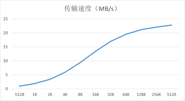
该模块通过了FPGA下的大量数据传输实测,速率测试方法是使用两个寄存器(传输周期数寄存器及传输字节数寄存器)并通过ILA采样,根据时钟周期换算得到的,因此精度非常高。下图是实测的传输速率曲线(从SD卡传输到DDR3,SD卡为TECLAST UHS-1 64GB卡),其中横坐标为单次传输的块大小,纵坐标为传输速率:
可以看到传输速率在块大小为512KB时达到峰值约23MB/s,,再增加块大小传输速率基本没太大变化趋于饱和,此峰值数值已经接近硬件电源(3.3V)和时钟条件(50MHz SDIO 4-wire)下的理论上限25MB/s(50MHz * 4bit = 25MiB/Sec)。
具体数据表如下:
| 数据大小(单位均为二进制Byte) | 传输速度(MiB/Sec) |
|---|---|
| 512B | 0.95 |
| 1K | 1.83 |
| 2K | 3.39 |
| 4K | 5.92 |
| 8K | 9.42 |
| 16K | 13.38 |
| 32K | 16.94 |
| 64K | 19.54 |
| 128K | 21.16 |
| 256K | 22.08 |
| 512K | 22.81 |
High-speed SD card controller based on AXI interface
A portion of the code from this project's sdcmd ctrl.sv and sd reader.sv files is referenced form the https://github.com/WangXuan95/FPGA-SDcard-Reader project andSD Specifications Part 1 Physical Layer Speicifcation Version 3.00 April 16, 2009
The SD card controller has the following features.
- operates in 50MHz SDIO 4-wire high-speed mode
- operates in the SD card multi-block transfer model
- transfer rates up to 23MB/s
- Active DMA on AXI4 interface (supports 256 bursts)
- AXILite configuration interface
- Supports up to 4GiB of data in one transfer
- Start sector up to 0xFFFFFFFF, i.e. access to any data in the entire range of the first 1TiB of the SD card
- Only read-only data be supported
The purpose of each file in the rtl directory is listed below:
| File name | Description |
|---|---|
| sdcmd_ctrl.sv | SDIO PHY layer, which implements the basic SDIO sequential logic |
| sd_reader.sv | SDIO MAC layer, which implements the basic command set and sector read control for SD cards |
| sd_controller_regfile.sv | AXILite controller register configuration interface and register implementation |
| sd_controller_ping_pong_buffer.sv | Ping/Pong Buffer |
| sd_controller_axi_writer.sv | AXI4 DMA which support write only 256 burst |
| sd_controller.sv | SD card controller top level layer |
| sd_controller_wrapper.v | Verilog card controller packaging |
The controller starts by outputting a 400KHz clock, a 25MHz clock after completing the basic SD card configuration process, and a 50MHz clock after switching to high speed mode.
To achieve such high-speed transfers, the controller uses Xilinx FPGA primes and constraints, with the primes partially implemented in a Verilog wrapper layer:
Highlight:
- BUFG converts the SD Reader's clock into a specialized FPGA clock network to optimize FF timing.
- ODDR is used to align the clock to the command output, among them the top ODDR is used to output the clock, and since D1 is connected to 0 and D2 to 1, ODDR will output a clock that is 180 degrees out of phase with the original clock, and since SDCMDOUT is changed at SDCLK, after the output clock is inverted, the Setup/Hold Timing of SDCMD relative to the output clock can be greatly improved to provide enough margin for the signal to be routed on the PCB.
- The SDCMDOE is tapped twice to align with the output SDCMDOUT signal and ensure that the tri-state gate is switched at the correct timing.
- SDCMDIN begins with tapped once on the FF of the IOB (where the signal now belongs to the sdclk_bufg clock domain), ensuring that the signal retains appropriate Timing margin after PCB alignment. Next, the signal from IOB FF is tapped again on LUT FF. The clock used at this point is aclk, the controller clock (100MHz in this case), to achieve a cross-clock domain. This approach is taken across the clock domain because sdclk_bufg is itself the generated clock for aclk. As a result, the synthesizer STA is able to accurately calculate Setup/Hold Time, which ensures that sub-stable problems, which typically arise across the clock domain, do not occur in this scenario.
- The SDDAT is a similar situation, first one tapped on IOB FF via sdclk_bufg and then one tapped with aclk, which is fed into the SDIO Reader.
The top-level module is sd_controller_wrapper, where the individual ports are described as follows:
| Port | Direction | Description |
|---|---|---|
| aclk | I | Controller clock (also AXI4 and AXILite clocks), must be 100MHz |
| aresetn | I | Controller reset signal (also as AXI4 and AXILite bus reset signal), active low |
| axilite_* | I/O | AXILite Slave configuration interface signal (configuration space size 4KB, both address data width 32bit) |
| axi_* | I/O | AXI4 Master DMA Write-Only interface signal (both address data width 32 bit) |
| sdclk | O | SD card clock line |
| sdcmd | I/O | SD card command line |
| sddat | I | SD card data line |
| card_type | O | SD card type signal |
| card_stat | O | SD card controller current status |
| interrupt | O | Interrupt signal, active high |
| test_* | O | For testing purposes only |
In order for the synthesizer to correctly calculate the STA across the clock domain, the following generation clock constraints need to be added (controller clock 100MHz, SDIO clock max 50MHz, set at 2 divisions):
create_generated_clock -name sdclk -source [get_pins top_design_i/clk_wiz_main/clk_out3] -divide_by 2 [get_pins top_design_i/sd_controller_wrapper_0/inst/sd_controller_inst/sd_reader_inst/sdcmd_ctrl_inst/sdclk_reg/Q]
where note that top_design_i/clk_wiz_main/clk_out3 need to be changed to the correct controller clock.
Currently tested on KC705 platform with FPGA XC7K325T-2FFG900, if you need to use other FPGA, please take care to replace the original language in sd_controller_wrapper.v.
The module can be used directly by Verilog or SystemVerilog or can be added directly to Vivado's Block Design for use.
An example software driver is available in the src directory which provides the following functions:
| Function | Description |
|---|---|
| sdcard_reset | Reset SD card controller |
| wait_sdcard_ready | Waiting for the SD card controller to be ready (timeout detection implemented, auto resent the command if timeout) |
| sdcard_read | Read SD card data, this function will wait for the SD card controller to be ready before initiating the command (timeout detection implemented, auto resent the command if timeout) |
| sdcard_is_busy | Returns TRUE to indicate that the SD card controller is busy |
| sdcard_get_progress | Get SD card controller progress |
For the timeout function to work, the user must populate the get_ms_time function in sdcard.c, which serves to range the system time in milliseconds.
Note that sdc need to be adjusted to point to the right SD card controller base address.
| Offset | Name | Properties | Description |
|---|---|---|---|
| 0x00 | CTRL | RW | Control Registers |
| 0x04 | STAT | RO(RW for INT) | Status Register |
| 0x08 | DSTADDR | RW | Target address |
| 0x0C | STARTSECTOR | RW | Starting sector |
| 0x10 | SECTORNUM | RW | Number of sectors (in 512 bytes, must be an even number) |
| 0x14 | PROGRESS | RO | Current progress (number of bytes) |
| 0x18 | RESET | RW | Reset Register |
RW - Read Write RO - Read Only
Control register:
| bits | Name | Description |
|---|---|---|
| 31:2 | Reserved | Always 0 |
| 1 | INT_EN | Interrupt (1 for enable, 0 for disable) |
| 0 | START | Start transmission (1 to start, reads constant 0) |
Status register:
| bits | Name | Description |
|---|---|---|
| 31:9 | Reserved | Always 0 |
| 8:5 | Card Stat | SD card controller state |
| 4:3 | Card Type | SD Card Type |
| 2 | INT | Interrupt hang (write 1 to this bit to clear the interrupt) |
| 1 | DMA Error | DMA write Memory send error |
| 0 | BUSY | In transit (1 means in transit, 0 means idle) |
The values and meanings of Card Stat are as follows.
| Value | Meaning |
|---|---|
| 0000 | CMD0 (GO_IDLE_STATE) command being sent, controller remains idle |
| 0001 | CMD8 (SEND_IF_COND) command being sent and waiting for response |
| 0010 | CMD55 (APP_CMD) command being sent and waiting for response |
| 0011 | ACMD41 (SD_SEND_OP_COND) command being sent and waiting for response |
| 0100 | CMD2 (ALL_SEND_CID) command being sent and waiting for response |
| 0101 | CMD3 (SEND_RELATIVE_ADDR) command being sent and waiting for response |
| 0110 | CMD7 (SELECT_CARD) command being sent and waiting for response |
| 0111 | CMD55 (APP_CMD) command being sent and waiting for response |
| 1000 | ACMD6 (SET_BUS_WIDTH) command being sent and waiting for response |
| 1001 | CMD6 (SWITCH_FUNC) command being sent and waiting for response |
| 1010 | CMD16 (SET_BLOCKLEN) command being sent and waiting for response |
| 1011 | Preparing to send the CMD18 (READ_MULTIPLE_BLOCK) command |
| 1100 | Waiting for response to CMD18 (READ_MULTIPLE_BLOCK) command |
| 1101 | Data being received from SD card |
| 1110 | CMD12 (STOP_TRANSMISSION) command being sent and waiting for response |
| 1111 | Waiting for the data reception state to reach the end of read state |
The values and meanings of Card Type are as follows:
| Value | Meaning |
|---|---|
| 0000 | Unknown type |
| 0001 | SD 1.0 |
| 0010 | SD 2.0 |
| 0011 | SDHC/XC 2.0 |
| 0100 | Maybe SD 1.0 card (only as intermediate, not as final state) |
| 0101~1111 | Reserved |
Target address register:
| bit | Name | Description |
|---|---|---|
| 31:0 | DSTADDR | Target address |
Starting sector register:
| bit | Name | Description |
|---|---|---|
| 31:0 | STARTSECTOR | Start sector (one sector is 512 bytes, do not exceed the SD card capacity range) |
Sector count register:
| bit | Name | Description |
|---|---|---|
| 31:23 | Reserved | Always 0 |
| 22:1 | SECTORNUM | Number of sectors (because 1KB of data is transferred at a time, the number of sectors must be even and cannot be zero, which is why the AXI burst is 256, 256 * 32bit = 1KiB) |
| 0 | Reserved | Always 0 |
Current progress register:
| bit | Name | Description |
|---|---|---|
| 31:0 | PROGRESS | Current amount of completed data transferred by DMA (bytes) |
Reset register:
| bit | Name | Description |
|---|---|---|
| 31:1 | Reserved | Always 0 |
| 0 | RESET | Write 1 to reset SD card controller, read constant 0 |
The module's accuracy is very high because it has been tested with a huge number of data transfers utilizing two registers (the transfer cycle count register and the transfer byte count register) and translated from clock cycles using ILA sampling. The following graph displays the measured transfer rate curve (from SD card to DDR3). The SD card used is a TECLAST UHS-1 64GB card, and the horizontal and vertical coordinates represent the block size and transfer rate, respectively:
It can be seen that the transfer rate peaks at about 23MB/s when the block size is 512KB. This peak value is close to the theoretical upper limit of 25MB/s (50MHz * 4bit = 25MiB/Sec) under hardware power (3.3V) and clock conditions (50MHz SDIO 4-wire).
The specific data table is as follows:
| Data size (Byte) | Transmission speed(MiB/Sec) |
|---|---|
| 512B | 0.95 |
| 1K | 1.83 |
| 2K | 3.39 |
| 4K | 5.92 |
| 8K | 9.42 |
| 16K | 13.38 |
| 32K | 16.94 |
| 64K | 19.54 |
| 128K | 21.16 |
| 256K | 22.08 |
| 512K | 22.81 |


