My TC Electronic M6000 does not boot anymore, I'm reversing the boot firmware in order to understand where it crashes.
Symptoms:
- Front panel led is still RED
- Internal leds are: on off off blink
- Floppy disk drive is never accessed (so it probably crashes before this part of the code)
As far as I understand, the M6000 mainboard is based on:
- an H8/3003 16 bits microcontroller
- with 2 SRAM chips (odd/even).
- an Intel 28F800 flash used to store the firmware
- a 93C46 SPI EEPROM (usage is still unknown)
The H8 is in charge of the boot process and control over the main bus used to communicate with the FPGA, the DSPs (over the bus connector) and the floppy disk drive controler. This repository is about the firmware reverse only, details on the electronics part can be found here: https://radix-studio.fr/blog/2022/03/10/going-deeper-on-the-m6000/
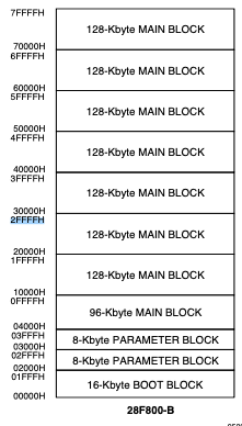
H8 boots on a E28F800 B5B70 memory chip. Since we're on x16 Mode / bottom boot, memory map is:
Since our firmware is 196608 bytes, thus 192KB (192*1024). This doesn't oubviously map to the memory map.
Another interesting point: the disassembly code starting from 0x00001C to 0xA617 is (almost) duplicated on 0x1001C to 0x1DDE7.
So our first main program ends near 0x10000 address (in 16bits mode) which is a 128KB memory zone (0x10000 * 2) (including around 44KB of padding). Our second main program also fits into a 128KB memory zone (0x10000 to 0x20000) . Starting from 0x20000 to the end at 0x2FFFF we have another 128KB memory zone, this time empty.
Our flash memory chip select is connected to CS0 on the H8 CPU.
When accessing the Flash chip (28F800):
- FLASH_CS is set to 0
- Address is set using A1-A20
- Value is read/written using D0-D15
When default dip switches settings is used, FLASH_CS is actually BOOT_CS and connected to H8 pin 104: CS0/P84 Port 8 direction can be set using register xFFCD, by setting bit 4 to 1. Port 8 value can be set using register xFFCF, byt setting bit 4.
When accessing the SRAM chips:
- SRAM_CS is set to 0
- Address is set using A1-A17
- Value is read/written using D8-D15
SRAM_CS is actually CS1_RAM and connected to H8 pin 103: CS1/P83
When accssing the floppy disk drive:
- FD_CS is set to 0
- Address is set using A0-A2
- Value is read/written using D8-D15
FD_CS is actually CS5_FLOPPY and connected to H8 pin 14: CS5/PC3
When accessing the PCMCIA port:
- PCMCIA_CS is set to 0
- Address is set using A0-A20
- Value is read/written using D8-D15
PCMCIA_CS is actually controlled in addition to PCMCIA_REG_CS by the FPGA.
| PIN | Label | Destination |
|---|---|---|
| P60 | "WAIT" | FPGA:BUS_ACK and PCMCIA:PCM_WAIT and FLASH:WAIT |
| P61 | "" | FLASH:P61 |
| P62 | "" | FLASH:P62 |
| P80 | "IRQ_FD" | FD:IRQ |
| P81 | "CS_PCM_REG" | FPGA:PCM_REG_CS +(?) FLOPPY:PCM_REG_CS |
| P82 | "CS_PCM_MEM" | Switch 1B to FPGA:PCM_BUS_CS OR Switch 1D to FLASH:FLASH_CS |
| P83 | "CS_SRAM" | MAX693 to "SRAM_CS" to FLASH:"SRAM_CS" |
| P84 | "CS_BOOT" | Switch 1A to "FLASH_CS" to FLASH:CS OR Switch 1C to FPGA:PCM_BUS_CS |
| P90 | "REM_TX" | ExternalItf:TXD0 (out) |
| P91 | "MIDI_TX" | ExternalItf:TXD1 (out) |
| P92 | "REM_RX" | ExternalItf:RXD0 (in) |
| P93 | "MIDI_RX" | ExternalItf:RXD1 (in) |
| P94 | "DCD0" | ExternalItf:DCD0 (in) |
| P95 | "HAND_S_REM" | ExternalItf:HAND_S_REM (out) |
| PC0 | "SEE_CS" | 93C46 EEPROM to EEPROM:CS (out) |
| PC1 | "SEE_CLK" | 93C46 EEPROM to EEPROM:CLK (out) |
| PC2 | "CS_BUS" | FPGA:BUS_CS (out) |
| PC3 | "CS_FLOPPY" | FLOPPY:FS_CS (out) AND FPGA:FS_CS (out) |
| PC4 | "CS_OPT_CS" | FLASH:OPT_CS (out) |
| PC5 | "SEE_DO" | 93C46 EEPROM to EEPROM:DO (in) |
| PC6 | "BUS_IRQ" | BUS_INTERFCE:BUS_IRQ (in) |
| PC7 | "PCM_IRQ" | PCMCIA:PCMCIA_IRQ (in) |
| PA0 | "FD_TEND" | FLOPPY:FD_TEND (out) AND FPGA:TEND (out) |
| PA1 | "X-DETECT" | J4:4/5V (in?) |
| PA2 | "SMPTE-IN" | ExternalItf:SMPTE_IN (in) |
| PA3 | "" | J4:3 |
| PA4 | "" | J4:2 AND LED4/ => Always on |
| PA5 | "" | LED3/ |
| PA6 | "" | LED2/ |
| PA7 | "" | LED1/ => blink182 |
| PB0 | NC | |
| PB1 | "SEE_DI" | 93C46 EEPROM to EEPROM:DI (out) |
| PB2 | "F_WP" | FLASH:F_WP (out) => "désactive la sécurité du boot block" |
| PB3 | "EN_485" | ExternalItf:EN_485 (out) |
| PB4 | "OE_485" | ExternalItf:OE_485 (out) |
| PB5 | "WATCH_DOG" | MAX693:WDI (out) |
| PB6 | "FD_DREQ" | FLOPPY:FD_DREQ (in) AND FPGA:FD_DREQ (in) |
| PB7 | "BATT_TEST" | battery |
| P70 | NC | |
| P71 | "-5V" | BUS_INTERFACE:-5V (in) |
| P72 | "V-BATT" | battery |
| P73 | NC | |
| P74 | "REM_VCC" | ExternalItf:REM_VCC (in) |
| P75 | "WP" | PCMCIA:WP (in) |
| P76 | "F_RY/BY" | FLASH:F_RY/BY |
| P77 | "PEDAL" | ExternalItf:PEDAL (in) |
