Working my way through the Nand2Tetris project & understanding the inner workings of a computer.
This project is from the course nand2tetris. From building logic gates to writing a high level language and an operating system in it, the resultant is a modern-day 16-bit computer which I have documented below.
Building a Modern Computer From First Principles.- Bare bones hardware - The _Hack_ computer
- Assembly language - The _Hack_ assembly
- Virtual machine - The _Jack Virtual Machine_ (JVM)
- High level language - The _Jack_ programming language
- Operating System - The _Jack_ OS
This section aims at building the bare-bones of the computer. We first make simple logic gates and then leverage them to further make more sophisticated hardware. The logic is written in a custom Hardware Description Language (HDL) specified here.
All the logic gates are created from the primitive Nand gate. Here are a list of gates that were implemented.
| Nand | Nor | Not | And | Or | Xor | Xnor |
|---|---|---|---|---|---|---|

|

|

|

|

|

|

|
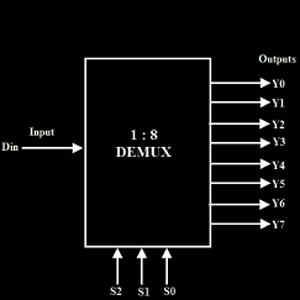
| Mux | DMux |
|---|---|
 |
 |
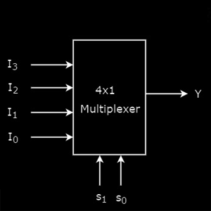
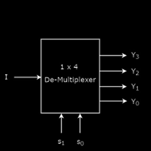
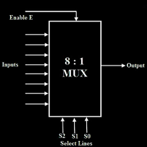
| Mux4Way16 | DMux4Way16 | Mux8Way16 | DMux8Way16 |
|---|---|---|---|
|
|
|
|
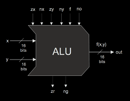
This ALU can compute eighteen functions using some minimal hardware design. It uses 6 control bits where each bit refers to a certain elementary operation.
| control-bit | description |
|---|---|
| zx | zero the x input? |
| nx | negate the x input? |
| zy | zero the y input? |
| ny | negate the y input? |
| f | compute x+y (if 1) or x&y (if 0) |
| no | negate the output? |
The following functions can be computed with the control bits as follows:
| # | zx | nx | zy | ny | f | no | f(x,y) |
|---|---|---|---|---|---|---|---|
| 1 | 1 | 0 | 1 | 0 | 1 | 0 | 0 |
| 2 | 1 | 1 | 1 | 1 | 1 | 1 | 1 |
| 3 | 1 | 1 | 1 | 0 | 1 | 0 | -1 |
| 4 | 0 | 0 | 1 | 1 | 0 | 0 | x |
| 5 | 1 | 1 | 0 | 0 | 0 | 0 | y |
| 6 | 0 | 0 | 1 | 1 | 0 | 1 | !x |
| 7 | 1 | 1 | 0 | 0 | 0 | 1 | !y |
| 8 | 0 | 0 | 1 | 1 | 1 | 1 | -x |
| 9 | 1 | 1 | 0 | 0 | 1 | 1 | -y |
| 10 | 0 | 1 | 1 | 1 | 1 | 1 | x+1 |
| 11 | 1 | 1 | 0 | 1 | 1 | 1 | y+1 |
| 12 | 0 | 0 | 1 | 1 | 1 | 0 | x-1 |
| 13 | 1 | 1 | 0 | 0 | 1 | 0 | y-1 |
| 14 | 0 | 0 | 0 | 0 | 1 | 0 | x+y |
| 15 | 0 | 1 | 0 | 0 | 1 | 1 | x-y |
| 16 | 0 | 0 | 0 | 1 | 1 | 1 | y-x |
| 17 | 0 | 0 | 0 | 0 | 0 | 0 | x&y |
| 18 | 0 | 1 | 0 | 1 | 0 | 1 | x|y |
The ALU also produces two status bits with the output.
| status-bit | description |
|---|---|
| zr | is the output zero? |
| ng | is the output negative? |
The following chips were implemented in this section
Future work: It will be better to replace the naive ripple carry adder in Add16 with a more efficient one like a carry-lookahead adder.
Storage is realized using Data Flip-Flops (DFFs). Registers are 16-bit wide and are composed of DFFs. These registers are further stacked to create the random access memory (RAM). It allows reading/writing data from/to any address in constant time, irrespective of the physical location.
Finally, a program counter is also realized using a 16-bit register which has the following functions - reset to zero, load a particular value, and increment the current value.
List of chips implemented
Bringing together all the circuitry, the computer is assembled in this section. The resultant device is a 16-bit von Neumann platform consisting of a CPU, two memory modules and two memory-mapped I/O devices - a screen and a keyboard.
There are two 16-bit registers A and D where D is the data register which intends at storing values, and A acts as a dual purpose register which can store both data and address. Depending on the instruction context, A's value can be interpreted as either data or a memory address. The A register allows direct memory access.
The complete instruction set reference is available at this. There are two generic types of instructions available - A-instruction or address instruction, and C-instruction or compute instruction. Each instruction has a binary and symbolic representation.
This is used to set the A register to a 15-bit value.
Instruction: @value
Binary: 0 v v v v v v v v v v v v v v v
A-instruction allows setting a constant value at a memory address. It also allows the C-instruction to manipulate a certain memory location or make a jump to a particular location. The left-most bit 0 is the A-instruction opcode and the following bits are the 15-bit value.
C-instruction accounts for all the compute tasks on this computer.
Instruction:dest=comp;jump // Either dest/jump maybe empty and symbols are omitted accordingly.
Binary:1 x x a c1 c2 c3 c4 c5 c6 d1 d2 d3 j1 j2 j3
The left-most bit 1 is the C-instruction opcode and the next two bits are don't cares. The comp field is specified by the a-bit and the six c-bits. The a-bit is responsible for selecting either A-register or Memory and the c-bits are the control bits for the ALU. The dest field is given by the d-bits which allow us to select a destination. Each bit is mapped to a particular location where data is written if the bit is set.
| d-bit | location |
|---|---|
| d1 | A-register |
| d2 | D-register |
| d3 | Memory |
The last three bits are the jump bits which decide when to make the jump. Together with the two status bits from ALU, they guide the PC in deciding the next address.
| j1 | j2 | j2 | Mnemonic |
|---|---|---|---|
| 0 | 0 | 0 | null |
| 0 | 0 | 1 | JGT |
| 0 | 1 | 0 | JEQ |
| 0 | 1 | 1 | JGE |
| 1 | 0 | 0 | JLT |
| 1 | 0 | 1 | JNE |
| 1 | 1 | 0 | JLE |
| 1 | 1 | 1 | JMP |
This computer has two memory banks - instruction memory and data memory. The instruction memory is implemented using a ROM chip with 32K addressable 16-bit registers. The data memory is a RAM device consisting of 32K addressable 16-bit registers with provision for memory mapped IO.
The data memory is laid out with the RAM in the upper section, followed by IO memory buffers for the two peripheral devices - a 512 x 256 display and a keyboard. Data memory supports 15-bit addressing.
| address | component | capacity |
|---|---|---|
| 0x0000 - 0x3FFF |
RAM | 16K |
| 0x4000 - 0x5FFF |
Screen | 8K |
| 0x6000 | Keyboard | 1 |
Implementation: Memory Chip.
The CPU consists on the ALU, two registers A and D, and a program counter PC. It fetches the instruction from the instruction memory and decodes it using internal circuitry of logic. It then executes the instruction and writes back the data.
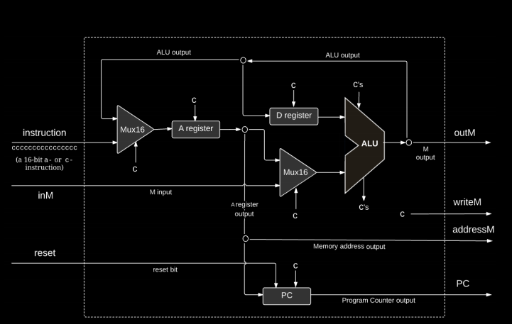
The control bits in the image above are labelled c. Different bits are routed to different parts of the CPU.
Implementation: CPU Chip.

