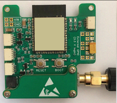
Last updated as of development iteration V1.5 (WIP)
(Add image of rear of assembled board with bracket screws like above)
(In the photos above, I use a SMA-female to SMA-male adapter as I wanted to prevent wear to the SMA connector on the board, as I didn't have any RP-SMA connectors nor antennas available at the time, see below for the reasons I prefer RP-SMA.)
This is an 8-layer board which uses JLCPCB's JLC08161H-2116 to base the controlled impedence calculations for the USB data lines. For 5 pieces the cost is less than $5 shipped due to their promotional offer, ordering mass quantities (400+) comes to approximately 1 USD each final effective price, but other manufacturering options are possible. This board focuses on being compact and portable, having a 50x50x9mm footprint with the antenna and power cable disconnected and no brace, and 50x50x12mm high with the brace. You can use the IPEX connector if you want to not take up a lot of space with an antenna attached directly to the SMA port. In this case it's best to not solder the SMA socket on so you don't accientally put two antennas at once.
The brace is to reinforce the USB-C connector as I kept snapping it off. I now use a surface-mount USB-C connector with holes acting only as allignment for the plastic nubs, and no TH metal, so the E22 module doesn't have solder underneath it.
Photos from the 3D render of EasyEDA Pro don't show the plating/solder mask (and epoxy fill) of vias. The actual PCB doesn't have holes where these 0.3mm and 0.4mm inner diameter vias are, and also has 'via-in-pad's.
You can now use the E22-900M33S for 2W output power (recommend for HAM-licenced operators ONLY), as well as any E22(0)-dddMddS which has the same footprint (so for example, not the E22-900M22S).
This board is capable of outputting a maximum of the module's claimed 30 dBm (Measured 29.8 to 30.1 dBm at 869.525 MHz using a tinySA, factoring in 60 dBm external attentuation, consisting of 3 separate pieces). Make sure you respect local regulations, more information, also regarding how the software works with the board, is in the variant.h file found in this directory. Check the output power of the E22-900M30S, albeit on a different board and at the default US frequency. Most notably, the power was measured from an additional IPEX connector that went through the board using a via, the actual power output is probably very slightly higher if using the on-board IPEX connector or a direct SMA connector on the same layer.
More information on CDEBYTE's modules can be found here.
RP-SMA is preferred even though it is less common in Europe, as it ensures there is no change of having a void connection between an SMA female board and RP-SMA male antenna. Also, with insertions the pin the slot end is worn more than the pin, it's easier to change antenna or antenna connector than replace the soldered connector on the board.
Especially if using the board SMA-style connector, use an bendable antenna, or one with a lead cable, as to enable the adjustment of the antennas orientation.
More tips can be found on the text of the schematic and PCB silkscreen, as well as the Document layer of gerber file.
Power
- Add extremely low drop reverse polarity protection if DC-DC output tantalum capcaitors are used and DC-DC IC doesn't already integrate it. Don't put tantalums on raw input :-D
- TPS63020 or TLV62569 for 5 to 5.2 V, ensure no noise at 2 A
- DC-DC for 3.3 V if no noise and reduces power consumption
- Battery charging, customisable current and voltage/battery type
- Battery protection
- Battery ADC voltage measurer which can be turned on and off to decrease power consumption in sleep
- DC-DC for ESP32 3.3 if noise is acceptable
- Use nRF52840 or nRF54 instead of ESP32 for reduced power consumption (we don't need Wi-Fi)
- Globally check which capacitors are actually needed and the optimal value for all
MCU
- Add RC delay circuit to MAX809T input voltage, or find a way to remove it completely and still turn on consistantly (not in hung state) when power is quickly cycled, or turned on when all capacitors are fully discharged.
- Add ESD protection IC on USB, USBLC6-2SC6
- Small capacitors between USB data lines and GND needed?
- Reduce I2C resistor values to 10 kΩ or something depending on if most I2C devices have resistors on them.
- Globally check which resistors are needed on UART, and if having two in series causes a problem or reduces max speed etc, including GPS
Radio module
- Add option to connect DIO2 to MCU pin to use it as an interrupt
- Can use E22-900M33S for 2 W - make sure the power limited is suitable for this power. Also can the RF switch isolate 2W? I don't think so. Will this damage the RX and LNA path?
- Make sure it's okay when TXEN and RXEN are both low, which path does the RF switch choose? It seems bad to use the same signals for RF switch control and PA and LNA control.
More improvements to implement may be listed on the schematic.
