All source code and images are associated with the paper:
"Current-controlled nanomagnetic writing for reconfigurable magnonic crystals" (2020),
Nature Communications Physics
(Accepted for Publication)
Paper HTML
Strongly-interacting nanomagnetic arrays are crucial across an ever-growing suite of technologies. Spanning neuromorphic computing, control over superconducting vortices and reconfigurable magnonics, the utility and appeal of these arrays lies in their vast range of distinct, stable magnetization states. Different states exhibit different functional behaviours, making precise, reconfigurable state control an essential cornerstone of such systems. However, few existing methodologies may reverse an arbitrary array element, and even fewer may do so under electrical control, vital for device integration. We demonstrate selective, reconfigurable magnetic reversal of ferromagnetic nanoislands via current-driven motion of a transverse domain wall in an adjacent nanowire. The reversal technique operates under all-electrical control with no reliance on external magnetic fields, rendering it highly suitable for device integration across a host of magnonic, spintronic and neuromorphic logic architectures.
Below is the schematic of the magnetic reversal method:
 Figure 1: (a) Representation of the ferromagnetic domain wall-carrying ‘control’ nanowire and ‘bit’ nanoisland, separated by a non-magnetic gap of height h. (b)–(d) Time-evolution series of the magnetic reversal process in two-nanoisland system. Both nanoislands are initially magnetized with 𝑀 = −𝑦̂ (b) before the current-driven ‘control’ domain wall (c-DW) traverses the right-hand nanoisland, inducing magnetization reversal (c), leaving it magnetized 𝑀 = +𝑦̂, whereas the left-hand nanoisland remains unswitched (d). It is noteworthy that the internal domain wall structure in (c) and (d) is slightly distorted by the drive-current; (b) shows the static, relaxed domain wall state. (e) Detailed time-evolution series of the reversal process in a single 400 × 75 × 5 nm3 nanoisland. The dynamic c-DW is represented by the white circle traversing the nanoisland midpoint, moving with 𝑣c−DW = +𝑥̂. t = 0 s is defined when the c-DW begins moving from its origin, 112 nm to the nanoisland’s left. The partially formed contorted nanoisland domain wall is highlighted in t = 0.6 ns by the dashed grey line, with the partially formed straight island domain wall highlighted by longer grey dashes in t = 0.65 ns. Topological defects are labelled with their winding numbers.
The simulations are developed using mumax3, a GPU-accelerated micromagnetic simulation program developed at the DyNaMat group of Prof. Van Waeyenberge at Ghent University. This is availabe at https://mumax.github.io/. In addition, the Object Oriented MicroMagnetic Framework (OOMMF) was used to generate two-dimensional simulations, some of which are presented as figures in the paper. See more detail at https://math.nist.gov/oommf/. Below are the simulations that were generated by running the provided scripts on the Imperial College London Research Computing Service:
(i) Selective reversal of single nanoisland in two-island system
- script name: simulation_1.mx3
- link: https://youtu.be/FiKxKtBjk7k
Description: Right-hand nanoisland in a two-nanoisland system is magnetically reversed while left-hand nanoisland is not reversed as the c-DW does not traverse it, demonstrating the local selectivity of the reversal method.
Reversal.Process.mp4
(ii) Fully-selective reversal returning arbitrarily magnetised four-island system to uniform state, then fully-reversed state
- script name: simulation_2.mx3
- link: https://youtu.be/F19qnYPWQKM
Description: Combination of two 'skip' followed by two 'write' events returns abitrarily magnetised system to a uniform state. The drive-current polarity is then reversed such that the c-DW motion is right-to-left, and a further combination of two 'skip' and two 'write' events are employed to prepare a state which is a total magnetic reversal of the initial arbitrary magnetisation state. Nanowire is in h = 20 nm fully-selective mode.
Selective.writing.-.Reversing.all.the.magnetisation.states.of.the.nanoislands.mp4
(iii) c-DW skipping across four-island system
- script name: simulation_3.mx3
- link: https://youtu.be/4WkLE20AFM4
Description: Four 'skip' events are combined to move the c-DW across a four island system without reversing any island magnetisation, demonstrating the freedom to reposition the c-DW throughout an array.
Selective.writing.-.Skipping.pass.all.the.nanoislands.mp4
(iv) Fully-selective reversal combining 'skip' and 'write' events to prepare a 'single gate' state
- script name: simulation_4.mx3
- link: https://youtu.be/x4G3z80CK_g
Description: Reversal method employing varying current-density pulses to achieve combination of 'skip' and 'write' c-DW traversal events in a four-island system. Nanowire is in h = 20 nm fullyselective mode. Starting from a uniformly-magnetised initial state, a combination of a single 'skip' followed by three 'write' pulses are used to prepare an arbitrary magnetisation state. The final state corresponds to a 'single gate' case, gated at the right-hand island.
magnetic.writing.single.gate.state.mp4
(v) Non-selective Oersted field reversal of both nanoislands in a two-island system
- script name: simulation_5.mx3
- link: https://youtu.be/-BJTMOu3GCc
Description: Both nanoislands in a two nanoisland system are simultaneously reversed by the Oersted field caused by current passing through the nanowire. This demonstrates the distinction between the c-DW reversal method described here and conventional, non-selective Oersted field stripline techniques.
Oersted.field.switching.magnetisation.of.nanoislands.mp4
(vi) Selective reversal of single nanoisland in two-island system c.f. (v)
- script name: simulation_6.mx3
- link: https://youtu.be/dsGObVhVJUc
Description: Right-hand nanoisland in a two nanoisland system is magnetically reversed while left-hand nanoisland is not reversed as the c-DW does not traverse it, demonstrating the local selectivity of the reversal method.
Switching.magnetisation.of.the.nanoislands.mp4
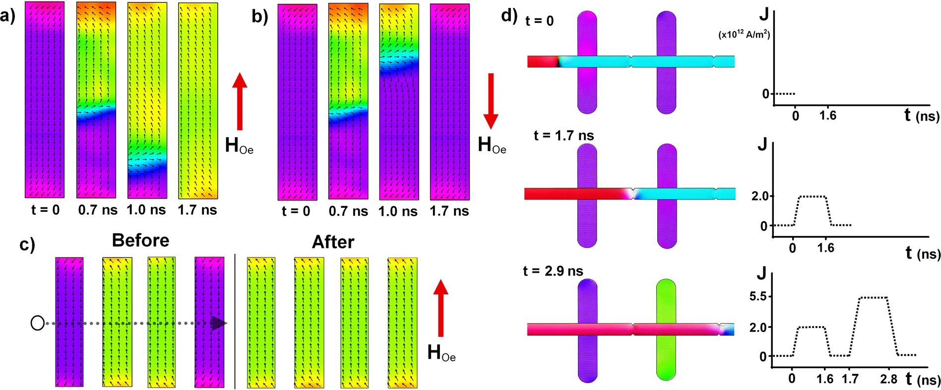
Two reversal modes were studied: (a) close-proximity, and (b) fully selective. See the figure below or refer to the paper for an in-depth discussion.
 Figure 2: Close-proximity and fully selective reversal modes. (a)–(c) Close-proximity reversal mode. (d) Fully selective reversal. (a) With Oersted-field HOe antiparallel to the initial nanoisland magnetization HOe aids reversal, driving the low- and high-energy nanoisland domain walls (i-DWs) to opposite nanoisland ends and achieving successful switching. (b) With HOe aligned to the initial nanoisland magnetization, the reversal process is hindered, HOe drives the low- and high-energy i-DWs into the same nanoisland end, resulting in failed switching. (c) Four-island array initialized (‘before’ panel) with second and third islands in 𝑀 = +𝑦̂ state, and first and fourth in 𝑀 = −𝑦̂ state. Control domain wall (c-DW) is then driven across the array such that 𝐇Oe = +𝑦̂, driving successful reversal of 𝑀 = −𝑦̂ islands (as described in (a)) and failed reversal of 𝑀 = +𝑦̂ islands (as in (b)). (d) c-DW begins to the left of two nanoislands (t = 0). It is driven over the first nanoisland by a J = 2.0 × 10¹² A/m2 ‘skip’ current pulse, leaving the nanoisland unswitched as HOe + HDW < HN, the nucleation field. The c-DW is then driven over the second nanoisland with a J = 5.5 × 10¹² A/m2 ‘write’ pulse, switching the nanoisland magnetization as HOe + HDW ≥ HN.
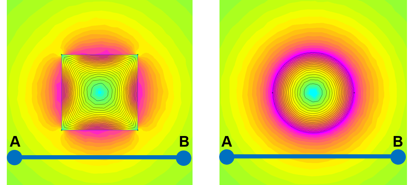
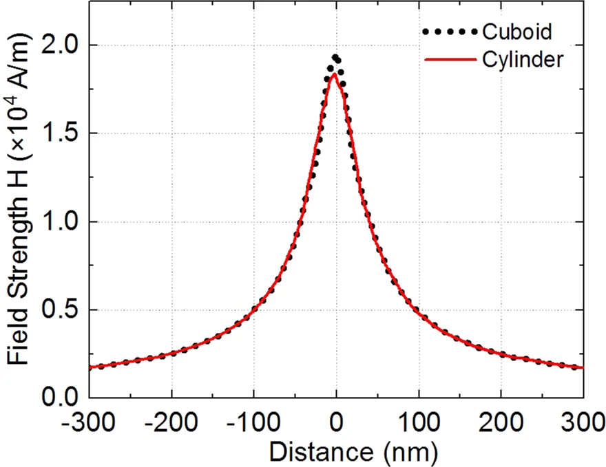
In our simulations, we have approximated the current-carrying wire as an infinitely-long cylindrical nanowire, as suppose to a cuboid nanowire. The rationale for such an approximation is due to the simplicity in modelling the magnetic field, which exhibit a circular pattern around a cylindrical nanowire. We have justified this approximation by computing the profile of the magnetic field strength experienced by the nanoislands, as shown below.
 Figure 3: Field profiles of current-carrying cylindrical and cuboid nanowires. The line joining Points A and B indicates the position of the nanoisland.
Figure 4: Field profile experienced by a nanoisland that is positioned h = 10 nm below an infinitely long cylinder and cuboid. There is a small discrepancy of 0.15 × 10⁴ Am-1 around x = 0, which can be minimized by adjusting the value of the current density.
ovf
-
Files with extension ovf such as 'init_grid_cDW_1.ovf' and 'init_grid_cDW_2.ovf' are Open Virtualization Format files. They are used to initialise the magnetisation state of domains in the current-carrying nanowire. They were generated by running 'grid_1.mx3' and 'grid_2.mx3', respectively. These ovf files are loaded to the mx3 file to avoid the initial minimisation step, reducing the run time and eliminating the randomness associated with the positioning of the c-DW while the system's energy is minimised. This is particularly useful when developing a simulations where there are many nanoislands and the c-DW is required to be on either the left or right side of the current-carrying nanowire, and not at the centre.
-
Simulations (ii) to (iv) utilises this method, where 'init_grid_cDW_1.ovf' is used in Simulations (ii) and (iii), and 'init_grid_cDW_2.ovf' is used in Simulation (iv).
mx3
- Files with extension mx3 are mumax3 simulation files that are used to generated the three-dimensional model of the proposed magnetic writing method.
pbs
- The file with extension pbs such as 'run.pbs' is a Portable Batch System file. This is used to submit the job the a High Performance Computer.
Gartside, J.C., Jung, S.G., Yoo, S.Y. et al. Current-controlled nanomagnetic writing for reconfigurable magnonic crystals. Commun Phys 3, 219 (2020). https://doi.org/10.1038/s42005-020-00487-y


