- Martin Ťavoda
- Vojtěch Drtina
- Jan Gadas
- Miloslav Kužela
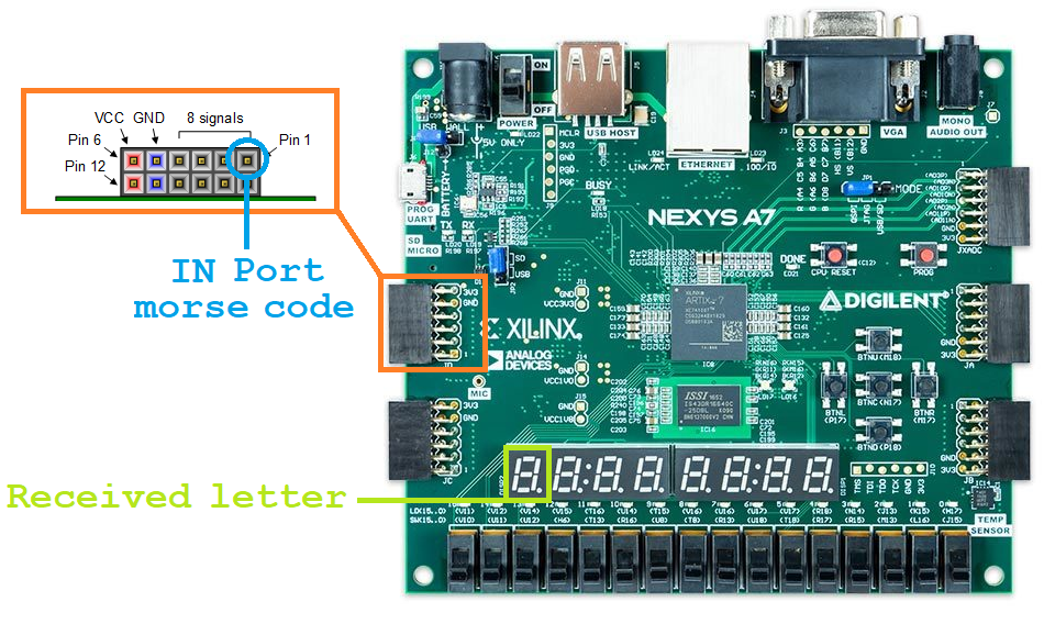
On the receiving FPGA board, the incoming letter is instantly displayed on 7-segemnt, without any need of user interaction.
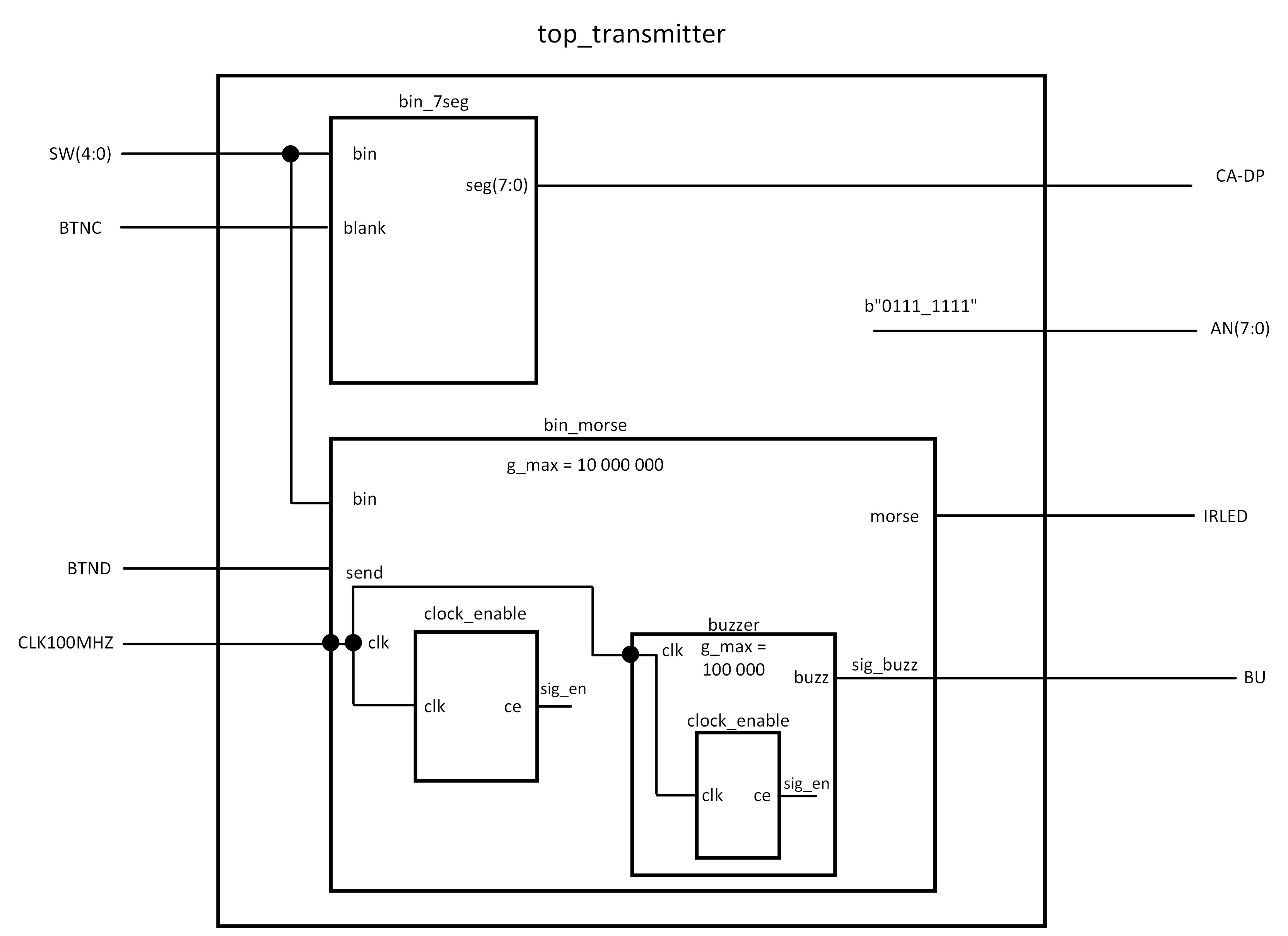
The top_transmitter has four input and four output ports. It includes two entities. Bin_7seg, which converts the input binary code to individual segment to be set on the display. The segment can be blanked by pressing a button (BTNC). The second entity (bin_morse) of top design is the main converter from binary format of letter to morse code. It contains the prescaler, which divide the main clock by g_max = 10 000 000. That means, the morse converter is controlled by clock with period of 100 ms. It also contains buzzer entity which generates PWM signal of duty cycle of 50% on 1kHz for external buzzer.
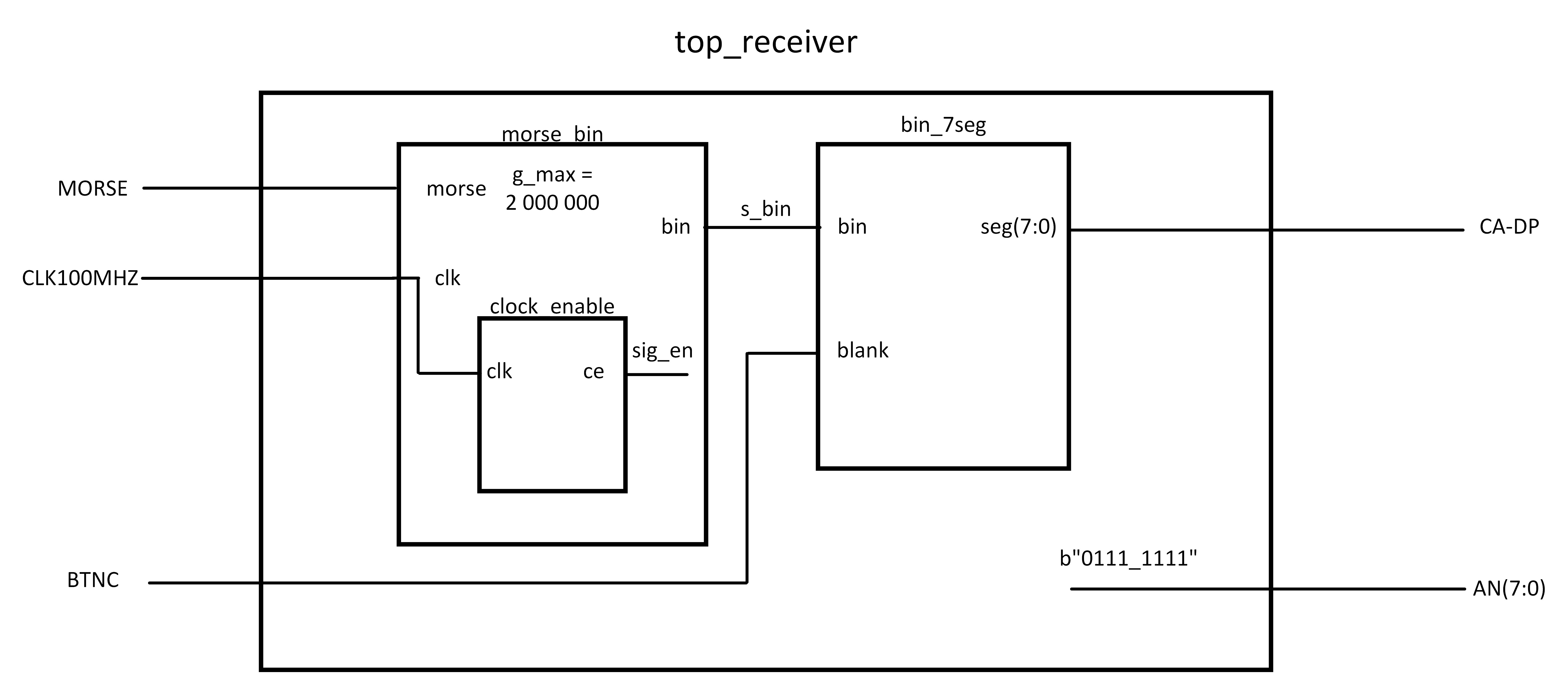
The software of receiving FPGA board is very similar to the transmitter. The top design source also contains two entities. First one, called morse_bin, parse the input morse code to bin representation of a letter. The conversion is done by decision of counter value, which is incremented during high pulse of input signal. If the value is 5 the input signal represents dot if it's 15 the signal represents dash. A low pulse is also followed by another counter, which when it reaches 200 ms, the reception of letter is considered as finished. All counters in this entity are feed by prescaler of constant g_max = 2 000 000, which coresponds to 20 ms.
The second part of top design is the same binary to 7 segment converter as in the transmitter.
Usage of the transmitter is as follows:
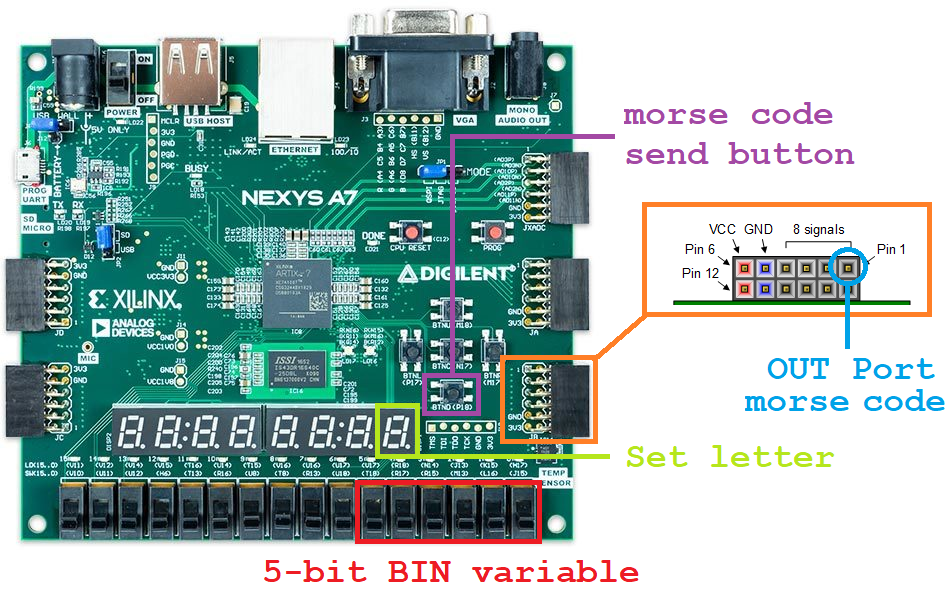
- By using position switches on the Nexys 4 Artix 7 FPGA development board, user can select a desired letter to be sent.
- BTND button serves as a send button. By pressing it, the transmitter sends the morse code to the receiver by an IR LED. The progress can be observed on an LED connected parallel to the sending output.
Receiver doesn't require any intervention by the user. It's always waiting for an incoming transmission and displays it on a 7 segment display.
- NEXYS A7 50T Reference Manual
- Digital electronics 1
- Falstad Circuit simulator
- own notes from lab exercises


