lorawan_eharvester_node
hardware and code artefacts of lorawan energy harvester node
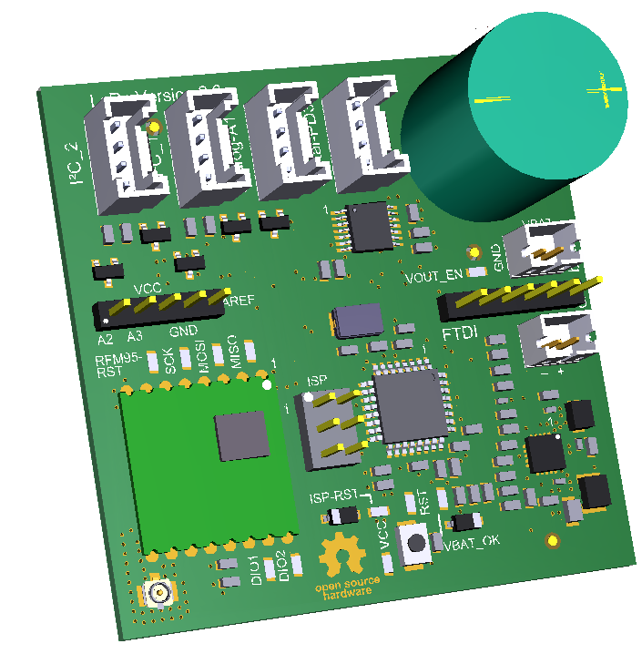
Technical features
- AVR ATmega328PB
- RFM95 LoRaWAN-Modul 868MHz (replaceable with other market variants)
- TI BQ25570 Energy Harvester with MPPT, configured for solar power source
- 1F Supercap
- 2x Grove I2C sockets
- 1x Grove Analog socket
- 1x Grove Digital socket
- 1x JST PH socket for battery connection
- 1x JST PH socket for solar panel connection
- 1x FTDI connector for serial console and programming
- 1x u.FL socket for LoRa antenna
- Power supply can be configured for different battery types (LiPo, LiFePo or similar)
- Switchable Vcc for Grove connectors through CMOS switches
- ISP socket for AVR programming
Sensor connections
In general all sensor sockets (Grove layout) have a switchable Vcc line. It is off by default and has to be enabled by corresponding GPIO lines.
I2C
There are 2 hardware I2C ports in the 328PB. Arduino currently supports one out of the box (running as a 328P Arduino Pro Mini clone). The second I2C port is prepared for future use.
Grove I2C 01
The SDA and SCL lines of the socket are connected to PC4 and PC5 accordingly.
GPIO PD4 == High (1) activates Vcc
When activating Vcc, additionally SDA and SCL are pulled high to Vcc via 10 kOhm resistors.
Grove I2C 02
The SDA1 and SCL1 lines of the socket are connected to PE0 and PE1 accordingly.
GPIO PD5 == High (1) activates Vcc
When activating Vcc, additionally SDA1 and SCL1 are pulled high to Vcc via 10 kOhm resistors.
Grove Analog
The analog signal connected to the socket is fed into the ADC1 input of the AVR.
GPIO PD6 == High (1) activates Vcc
Grove Digital
Vcc on the digital Grove socket is permanently supplied.
GPIO PD3 == Data input for digital sensor
Energy harvesting power supply
The Energy Harvester integrates a harvesting power supply chip BQ25570 from Texas Instruments. It provides the 3.3V Vcc supply voltage for the AVR and attached sensors. It also provides the charging voltage for the batteries and the supercap. It also features MPPT (Maximum Power Point Tracking), to extract maximum energy from solar panels even in low light scenarios. Other power sources like thermal energy generators (TEG) can also be adapted as power source. 5.5V is the maximum allowed charge voltage level of the BQ25570. And the maximum input voltage of the power source is 5.1V. The allowed peak input power is 510mW, thus a solar cell for this energy harvester should be selected accordingly and cells > 0.5W seem not to be feasible. A better approach would be to use two 0.25W cells in parallel to adapt to the sun path by pointing into different directions. Then, bypass diodes might have to added to the solar cells.
Product page: http://www.ti.com/product/BQ25570
Configuration of battery type
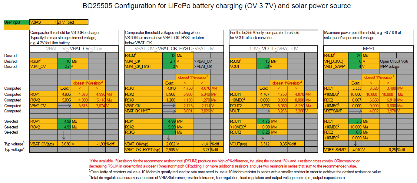
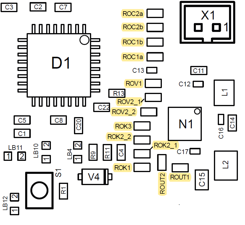
The image shows a resistor configuration sheet (example of LiFePo configuration), provided as a template by Texas Instruments. The sheet references the predecessor BQ25505, which provides the same configuration system with multiple resistors. All resistors are 1% 1/10W SMD parts in size 0603.
To configure the harvester for LiPo or LiFePo battery cells the corresponding resistors have to have the following values. This mainly adjusts the overvoltage level.
Info for Supercap mode: I'm currently trying out a Vishay supercap with 90F capacity at 5V. This will not have a backup battery. Idea is to increase overvoltage level to 5V (instead of 4.2/3.6V), to have more headroom for the Buck converter to longer provide 3.3V to the sensor electronics. Hopefully this is a solution for sensors that really need stable 3.3V supply. The LiPo/LiFePo configurations are running until below 3V. This currently is an untested resistor configuration!!!
| Part | Li-Po cells | LiFePo cells | Supercap mode |
|---|---|---|---|
| ROK1 | 4.99 MOhm | 4.99 MOhm | 4.22 MOhm |
| ROK2_1 | 3.3 MOhm | 4.99 MOhm | 4.02 MOhm |
| ROK2_2 | 4.02 MOhm | 1 MOhm | 3.3 MOhm |
| ROK3 | 806 kOhm | 1 MOhm | 681 kOhm |
| ROV1 | 5.62 MOhm | 4.99 MOhm | 3.6 MOhm |
| ROV2_1 | 4.02 MOhm | 4.02 MOhm | 3.0 MOhm |
| ROV2_2 | 3.3 MOhm | 1 MOhm | 3.3 MOhm |
| ROC1a | 3.3 MOhm | 3.3 MOhm | 3.3 MOhm |
| ROC1b | 10 MOhm | 10 MOhm | 10 MOhm |
| ROC2a | 1 MOhm | 1 MOhm | 1 MOhm |
| ROC2b | 5.6 MOhm | 5.6 MOhm | 5.6 MOhm |
Tracking of Vcc
Using a voltage divider Vcc is measured against the AVR internal reference voltage (1.1V, selected via Software, AVR reference "INTERNAL"). The corresponding voltage is fed into ADC0 of the AVR, to allow for a dynamic adjustment of the sleep interval, related to the actual Vcc voltage level. The lower Vcc the longer the sleep intervall to safe power. Vcc can only be measured, while analog Grove port is activated by GPIO PD6 == High.
PCB Bring Up
Test of Boost function
- Connect a 3V to 4V power supply with the solar connector X1, simulation a solar cell.
- Measure the open circuit voltage at the battery connector X2, which shall be the configured Overvoltage level
- After connecting a power supply it may take about 1 minute to charge the 1F supercap to the corresponding voltage level 4.2V, 3.6V or 5V
- Now connect a battery or a supercap, depending on build variant, that is compatible to the measured voltage level
Test of Buck function
- Set VOUT_EN active by bridging the corresponding jumper pads
- Measure voltage Vcc at 5-pin header and expect to see ca. 3.3V
Programming of Arduino bootloader
- Set VCC active by bridging the corresponding jumper pads
- Set ISP_RST active by bridging the corresponding jumper pads
- Connect the ISP adapter (z.B. ATMEL JTAGICE3) with the programming port
- Program a matching Arduino bootloader into the AVR
Fuse Bits
After programming the bootloader, we have to set the fuse bits to match the hardware features.
| Fuse | Value |
|---|---|
| CFD | "CFD_DISABLED" |
| BODLEVEL | "DISABLED" |
| RSTDISBL | unset |
| DWEN | unset |
| SPIEN | set |
| WDTON | unset |
| EESAVE | set |
| BOOTSZ | "256W_3F00" |
| BOOTRST | set |
| CKDIV8 | unset |
| CKOUT | unset |
| SUT_CKSEL | "EXTXOSC_8MHZ_XX_16KCK_14CK_65MS" |
These flags evaluate to the following bit masks:
EXTENDED= 0xF7 HIGH = 0xD6 LOW = 0xFF
Enable Reset lines
- Set RESET active by bridging the corresponding jumper pads
- This enables reset per switch and Arduino serial adapter (e.g. FTDI USB2COM)
- Set VBAT_OK active by bridging the corresponding jumper pads
- This enables reset by power good signal from bq25570 going low in case of battery undervoltage
Test of serial connection
- Connect a serial adapter
- Compile and download a simple Arduino sketch for the 328PB and check for valid debug output in serial console of Arduino
- This checks for a working serial port and a functioning bootloader
Connecting RFM95 I/O
Bridge the remaining jumper pads for the LoRa module, which are RFM95-RST, MISO, MOSI, SCK, DIO1 and DIO2.
Now you can adjust the supplied test sketch in the /src folder by adding valid keys for your TTN application into, compile and download it to the harvester. In the serial console you will find debug output after restart, giving information on the LoRaWAN communication.
Software
Configuration of Arduino IDE
Avrdude has to be configured to ignore the changed chip ID of the AVR ATMega328PB when uploading a new Arduino sketch. This is done by adding a '-F' to the command line options of verbose mode for avrdude in Arduino's platform.txt document. There are two lines to edit. After this activate "verbose" mode for upload in the Arduino IDE preferences.
tools.avrdude.upload.params.verbose=-v -F
tools.avrdude.program.params.verbose=-v -F
Libraries from Library manager inside Arduino IDE
The following libraries are needed to use the provided template sketch
- Low-Power by Rocket Scream Electronics (there are alot others with a similar name, please take this one)
- MCCI LoRaWAN lmic Library (tested with v3.0.99, currently the MCCI lmic version is the newest fork)
Additional libraries
https://github.com/felias-fogg/SoftI2CMaster
Board selection
Install the Arduino AVR Boards package and select "Arduino Pro or Pro mini" as board. As processor select "ATmega 328p (3.3V, 8MHz)". Now connect your FTDI TTL serial port and configure the port inside the IDE accordingly.
Example sketch for Arduino
The example sketch soil_humidity_sensor_template.ino in the /src folder presents a template for building a first prototype of the Energy Harvester with a capacitive soil humidity sensor attached.
Device and App configuration
Energy sources
Solar cells
crystaline solar cells
thin film solar cells
Measurements
Run and Sleep current
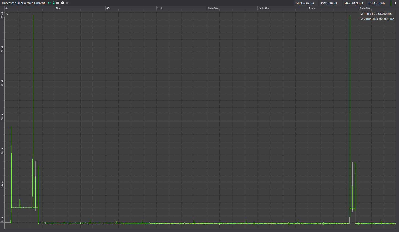
I made some test measurements with a Qoitech Otii source meter for sleep current of the energy harvester. These first measurements were done without attached external sensors, to see the theoretical minimum consumption of the node. It was measured at the battery port of the harvester and the supply was set to 3.2V, to simulate a LiFePo battery.
This is a recording of the system startup showing all power modes of the device. The peak current seems to be slightly above 60mA
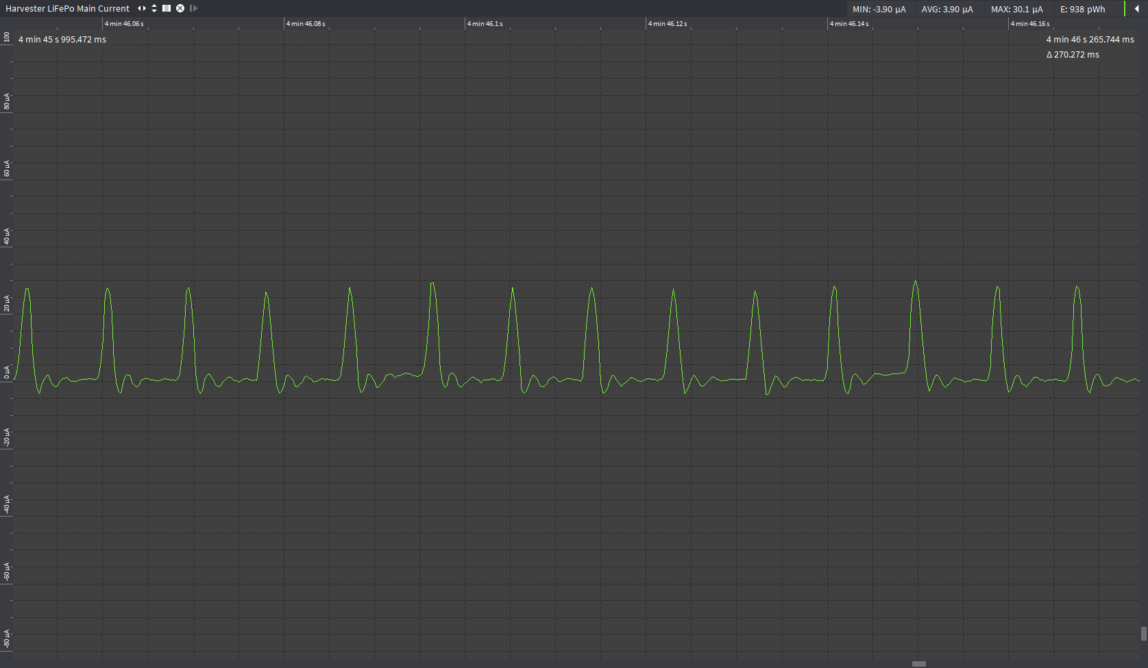
A zoomed view of sleep current. The internal power consumption of the BQ25570 seems to be visible here. We got a mean value of 3.9uA and a maximum value of 30.1uA sleep current.
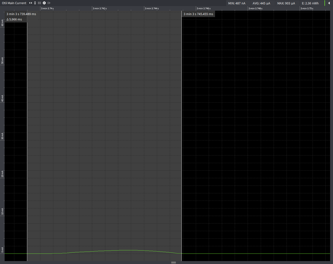
An even more detailed look into the energy consumption of the device when it wakes every 8s and going to sleep directly again. 8s is the longest possible sleep duration of the AVR internal sleep timer. So every longer sleep period has to be implemented with a sequence of a multiple of 8s sleeps. The ingrease of energy consumption for this "useless" sleep/wakeup is about 2.36nWh per iteration.
If you plan to use an external RTC to allow for longer sleep times and interrupt driven wake up, check if you RTC consumes less than the energy needed by a sequence of multiple 8s wake ups.
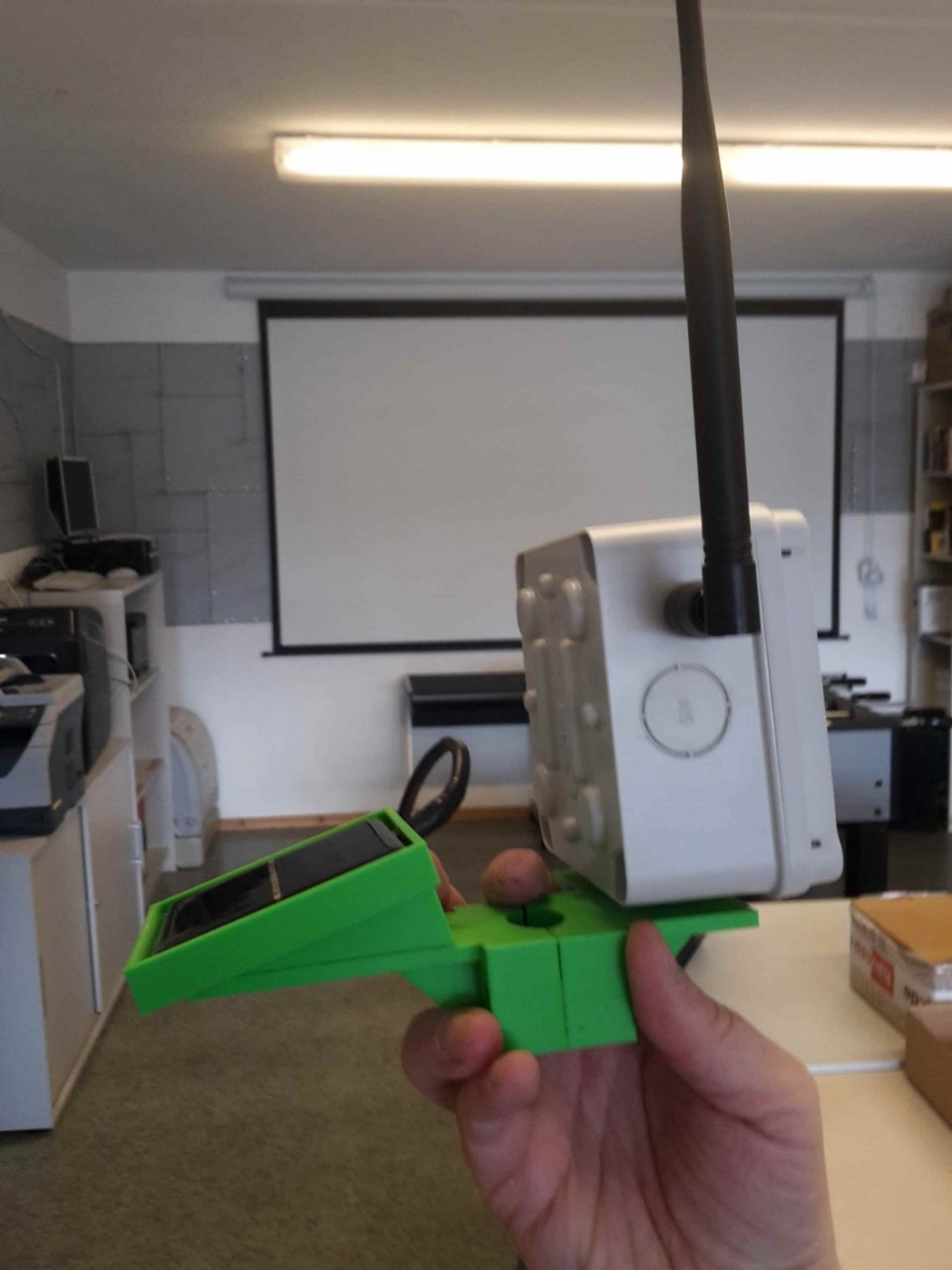
3D printed parts
There are also 3D print parts that help mounting the harvester in rugged outdoor housings