Enchanté is my personal PCB business card. It has been designed to show some of my skills while looking for a job.
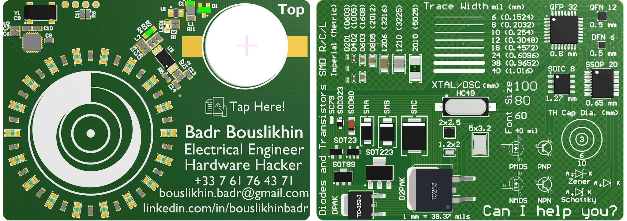
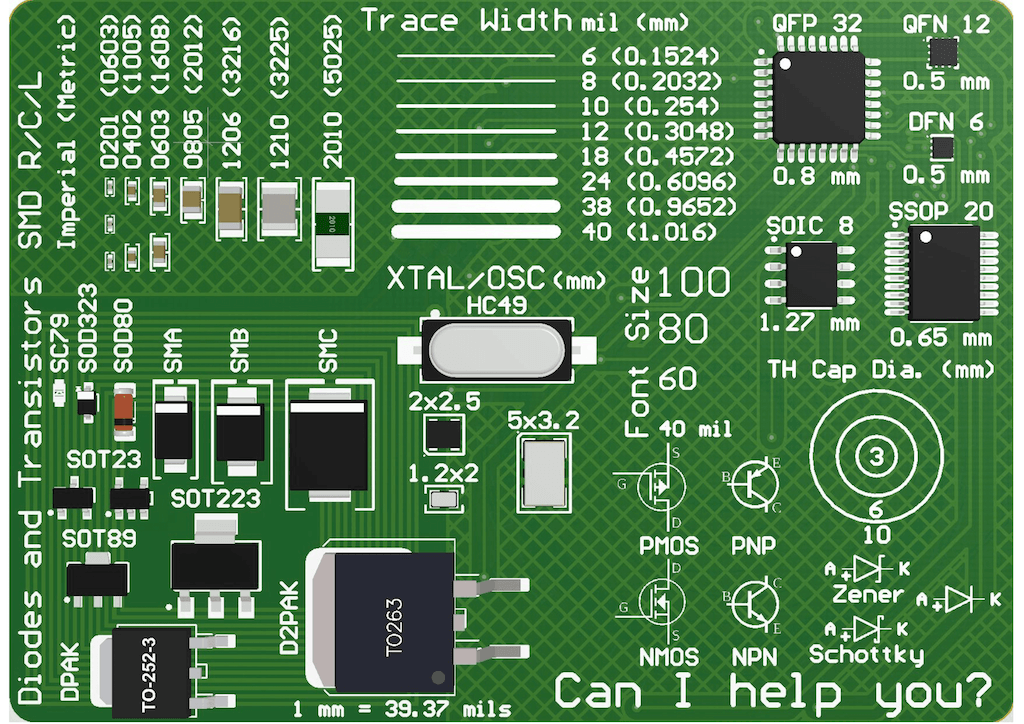
The small board (77 x 55 mm) features a capacitive touch sensor (iPod wheel style), some LEDs for animation and interaction with the touch sensor and an NFC chip with an onboard PCB loop antenna. The NFC will opens the browser with my LinkedIn profile and add my contact info the phone's address book. The bonus feature is a PCB reference on the back of the board (only footprints, no component will be soldered) with:
- Resistor/capacitor/inductor/diode footprints
- Common surface mount component footprints
- Common electrical symbols
- Common conversions
- Trace size comparison
- Font size comparison
Hopefully this will be useful for EEs and will save this business card from ending up in the trash.
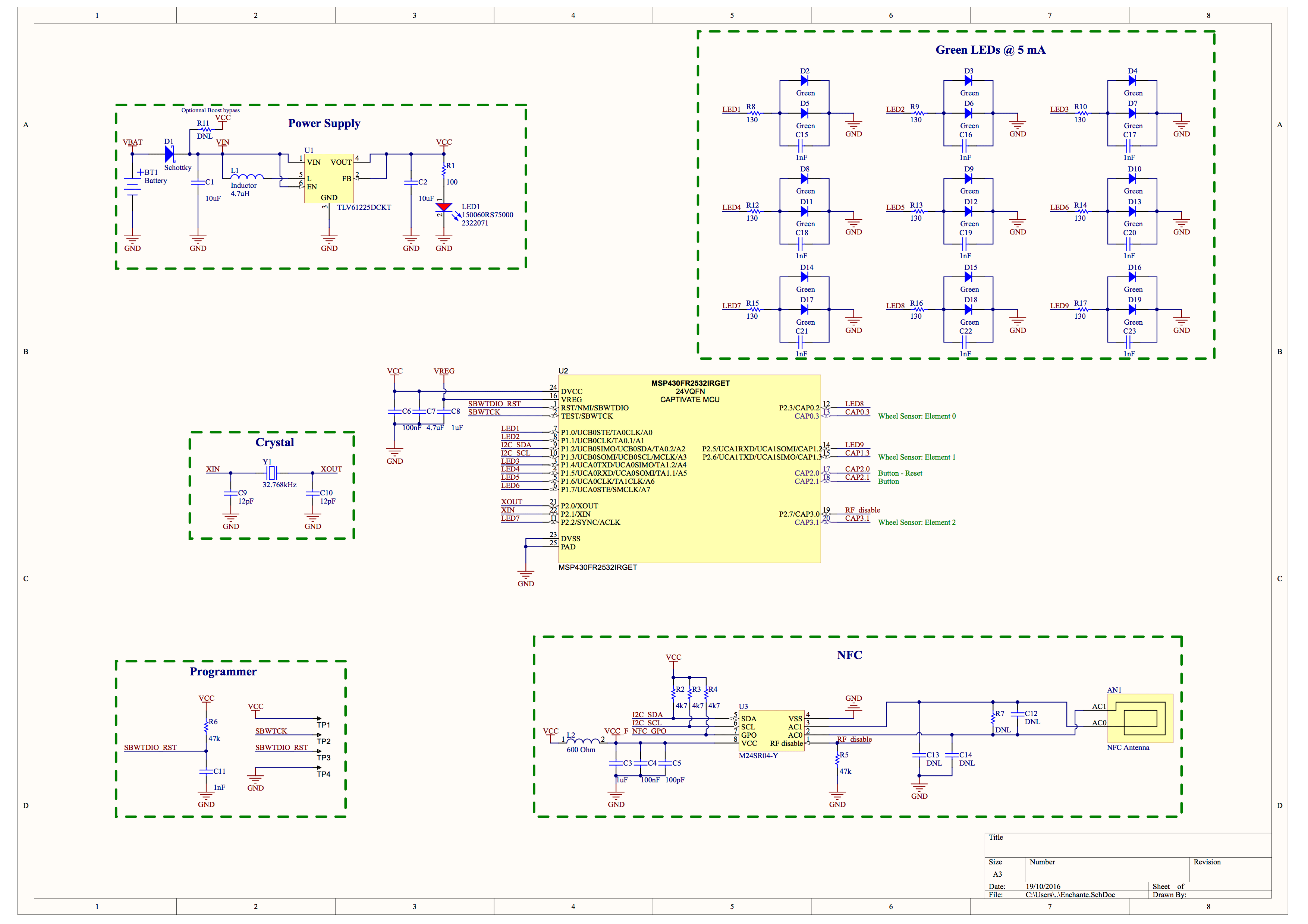
A TI MSP430 microcontroller with CapTIvate touch technology capability handles all the touch functionalities and LED control. There is a connectorless programming adapter. Just a few exposed pads to do all the programming without having pin headers onboard, this makes the card much easier to carry around.
The board is powered by a 3V CR2032 coin cell battery. A Boost converter is available to provide a stable 3.3V over the battery’s operating range. This enables energy-harvesting and optimizes the power efficiency.
This board is also a playground for me to learn about technologies I'm not familiar with, specifically NFC. The first version of this business card is very expensive. For ten units, the total cost per board is ~11.6$ and can be as low as ~10$ if the boost converter is not populated (which is possible in the schematic). The BOM cost is ~8$ and the PCB is ~3.6$ (ordered on Elecrow). A detailed BOM is available here. One of the goals for the next iteration would be to make it much cheaper.
This repository contains the hardware sources of the board. Although made with Altium Designer, the schematic is available in PDF and the layout is available in Gerber. I do not plan to convert the files to KiCad/Eagle at the moment but there are some converters you can use.
Enchanté
├── Antenna generation -- OpenSCAD scripts to generate the DXF of the NFC loop antenna
├── Board shape -- OpenSCAD scripts to generate the DXF of the board's shape
├── Enchante.OutJob
├── Enchante.PcbDoc -- PCB Layout
├── Enchante.PrjPcb
├── Enchante.PrjPcbStructure
├── Enchante.SchDoc -- Schematic
├── Images -- Images for the README
├── Librairies -- Altium component libraries
└── Project Outputs for Enchante
    ├── Enchante.pdf -- PDF Schematic, layout 2D/3D view
    ├── Enchante_BOM.xls -- BOM
    ├── Gerber -- Gerber fabrication files
    └── NC Drill -- Drill fabrication files
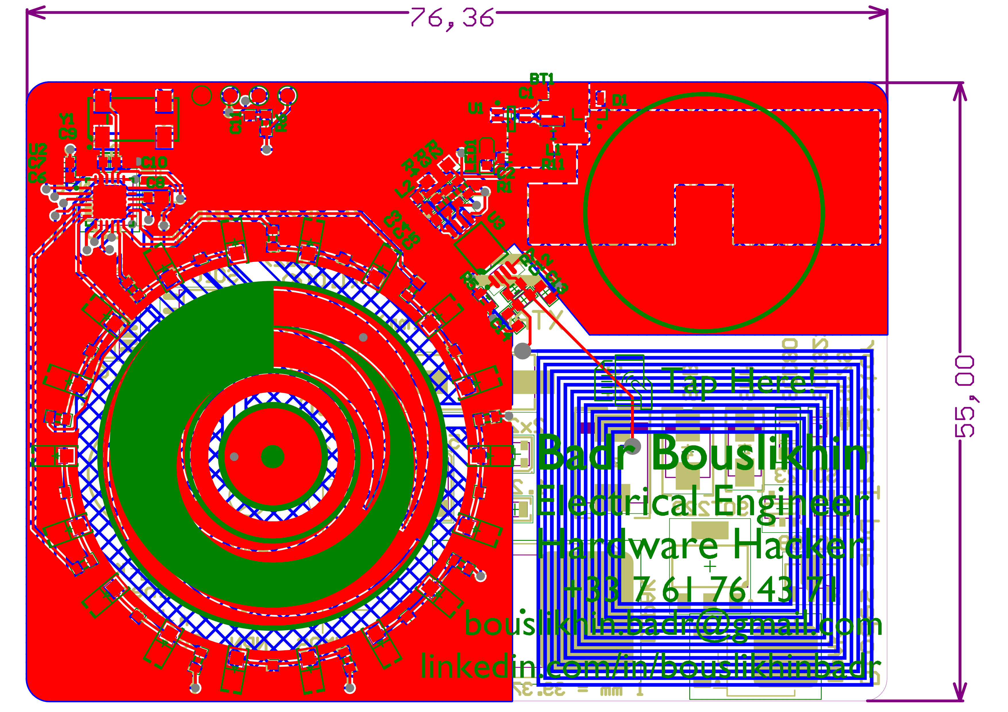
- Green: top overlay
- Red: top copper
- Blue: bottom copper
- Yellow: bottom overlay
NFC (radio-frequency identification) tags extract all of their power from the reader’s field. The tags’ and reader’s antennas form a system of coupled inductances. The loop antenna of the tag (this board) acts as a transformer’s secondary. The design principle of the NFC antenna is simple: the external antenna inductance (Lantenna) that needs to be designed on board the PCB should match the NFC chip internal tuning capacitance (Ctuning) in order to create a circuit resonating at 13.56 MHz:
![]()
The full equations are available in ST's application notes AN2972 and AN2866 and TI's application note SLOA197.
The antenna fine tuning is done by adjusting the antenna resonance frequency. The parallel capacitors C12 is added to bring the resonance frequency close to 13.56 MHz. C13 & C14 are part of the matching network.
A resistor R7 is added to tune the Quality factor if needed (should be Q < 50).
In this case, the calculated target inductance is 5.398 uH.
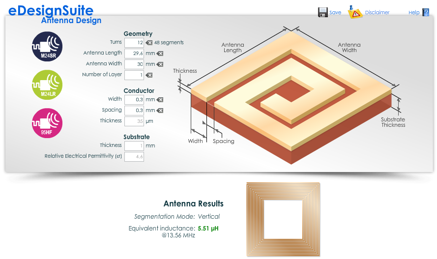
The next step is to choose the shape of the antenna and determine its physical dimensions. A rectangular loop seems to be the usual shape for this type of design. ST provides an online tool to help with the math:
 Now we need to create the component in the ECAD software (Altium Designer in this case). I was very surprised to find no integrated/easy way to do this. My workflow for this step is as follows:
- Create a DXF with the above geometry
- Import the DXF in Altium Designer, add vias and create a component
To create the DXF with this geometry, I wrote an OpenSCAD script to handle the job. It takes the following parameters and generates an STL of the desired geometry:
// Geometry
loops = 12;
length = 29.6;
width = 30;
copper_width = 0.3;
copper_spacing = 0.3;
thickness = 0.03556;
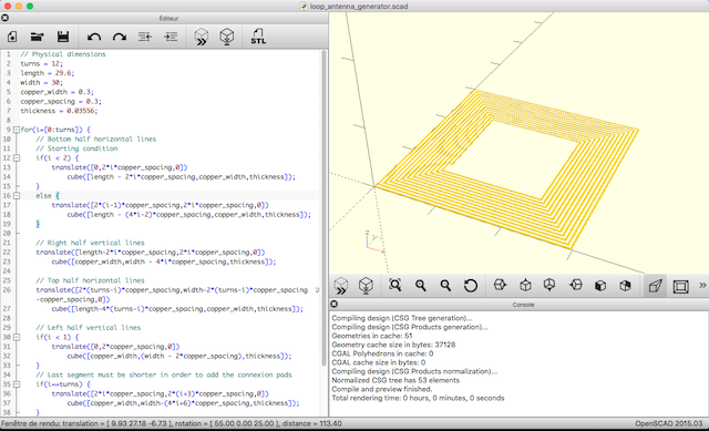
The next step is to convert the STL to a 2D object and generate a DXF, this is handled by another OpenSCAD script. The DXF is then imported in Altium Designer and the component is created by adding two vias to both ends of the antenna. The result in this Altium Integrated Library. This is maybe overcomplicated, if you find a better way of doing it, please shoot me an email!
There should be no copper near and especially under the antenna! I used a Polygon Pour cutout on both layers to keep the polygons pours from the desired region.
Capacitive sensing performs a measurement to detect a capacitive change to a sensor element. A sensor element can be any conductive material (copper PCB plane, a wire, etc.) and the change is due to human interaction, such as a finger, ear, or hand. A touch causes the capacitance of the electrode to increase (typically 1-10pF). Although expensive, the TI MSP430FR2532 microcontroller features CapTIvate touch technology for buttons, sliders, wheels (BSW), and proximity applications. This MCU has hardware blocks dedicated to this measurement hence making it much easier for me.
This technology uses Charge transfer technique to measure a change in capacitance. Since we are interested in the change in capacitance and not the absolute value, the basic principle of this technique relies on a charge transfer between two capacitors: an unknown capacitor Ctouch we are trying to monitor and a know capacitor Cref (larger enough, ~ tens of pF). Ctouch is filled (charged) and then emptied (transferred) into the Cref. The number of times it takes to fill the Cref is representative of the capacitance of the Ctouch. If the number of times it takes to fill Cref changes, then the capacitance of Ctouch has changed. Further information can be found in TI's CapTIvate™ Technology Guide.
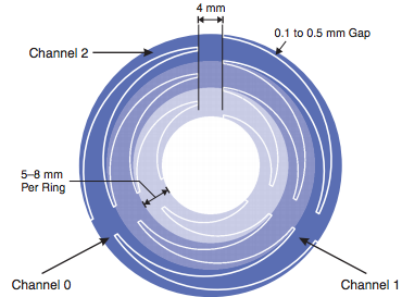
I chose to implement a wheel and a touch button in the middle. The first complexity of this type of implementation comes from the design of the sensor. In this case I used a spatially interpolated wheel with 3 electrodes connected to 3 different sensing channels of the MCU.
The geometry is not trivial to draw in ECAD software. There are few options to do so:
- Use OpenSCAD again and import the DXF into Altium to create the component. This approach has been realized in this design.
- Use Atmel's touch library add-on to Altium.
- Copy paste the sensor from TI's CapTIvate reference design.
The lazy me chose the third option. I only resized the component to meet my needs.
The other touch electrode is a simple button consisting of a copper pad and a via to connect it to the MCU. This one was easy to implement.
Ground planes are necessary to shield the design and protect it from radiated and conducted interference. This is conflicting with the need to minimize the parasitic capacitance (the sensor's sensitivity increases with the decrease of the parasitic capacitance) between the electrode and the ground pour. This is why on the bottom layer, the ground pour is hatched.
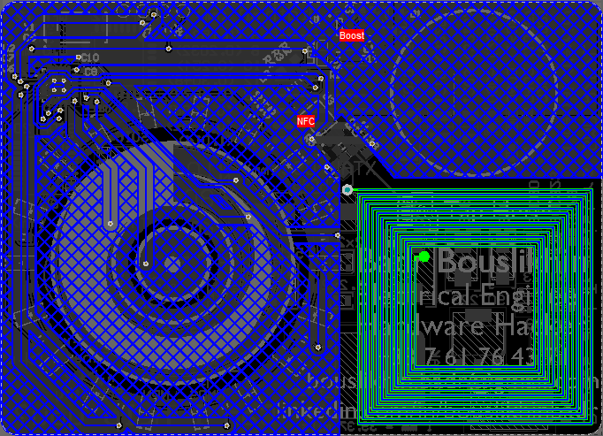
It is also recommended leaving 4 mm between the capacitive touch trace and any digital signal/ground pour to minimize coupling.
Done
The boards work perfectly! More details to come here.
Done
Code and details coming soon!
For any further information or inquiry, shoot me an email bouslikhin.badr[at]gmail[dot]com