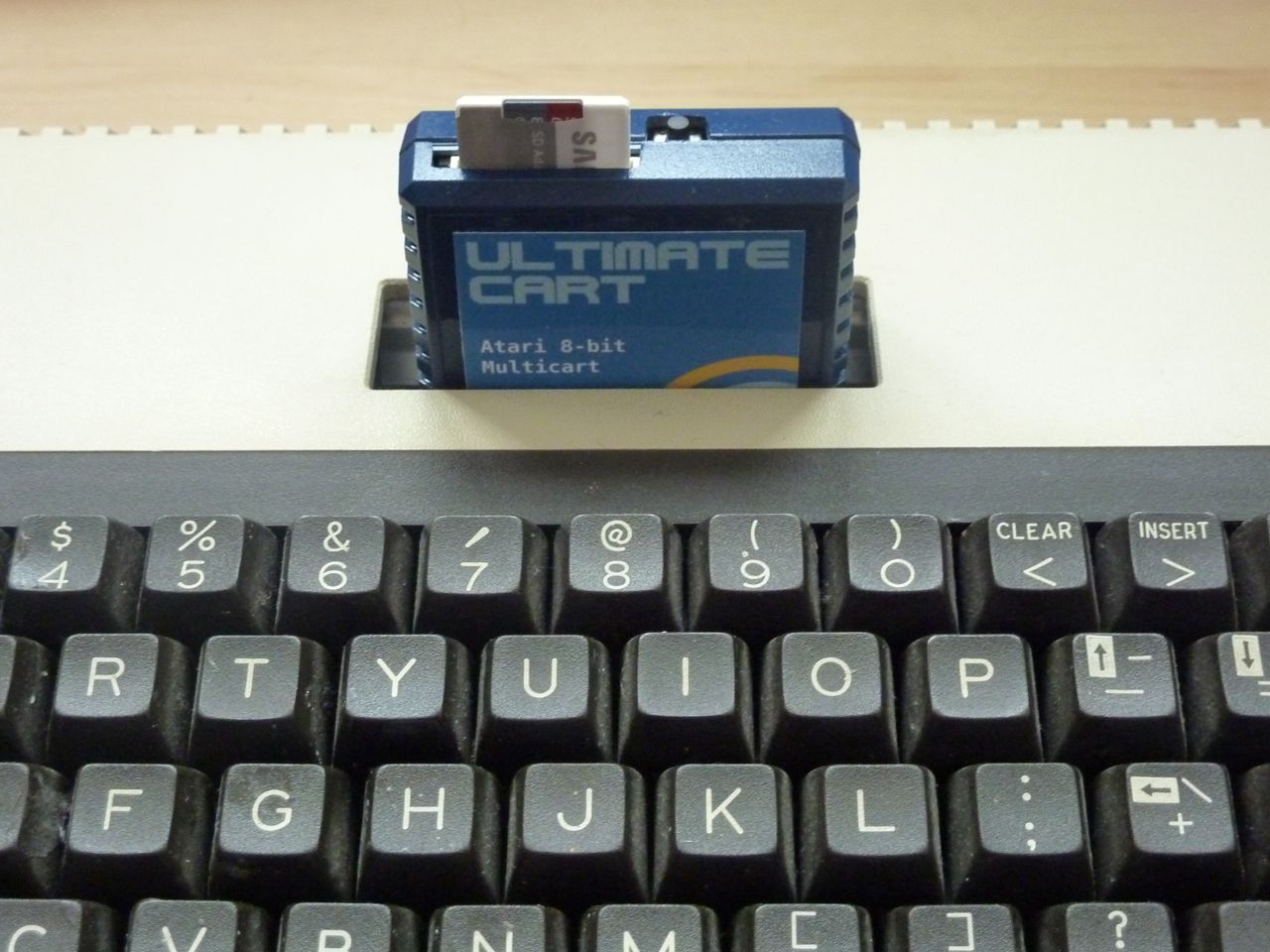
The Ultimate Cart is an SD-card based multicart for the Atari 8-bit, which I've been developing for the last few months. It allows you to browse the SD card on the atari and launch cartridge images from ROM and CAR files from the menu. The PCB is designed to fit in a standard grey cartridge case (after a bit of modification with some clippers and a file).
It supports most ROMs up to 1 megabyte in size, including standard 8k and 16k cartridges, XEGS, AtariMax 1 & 8mbit ROMs, SIC! Cart, Bounty Bob, OSS, SDX & Williams. ROM dumps can be easily converted into CAR format with my html/javascript conversion utility, RomToCar.
New firmware also allows XEX files (Atari executables) to be launched direct from the SD card.
The FPGA originally used was an engineering sample (ES) variant of the chip. The production version of the FPGA is now available and can be used instead. The programming files for the ES seem to work fine on the production chip.
1 x PCB (eagle .brd file can be uploaded to e.g. OSH park)
1 x Altera 10M08SAE144C8G or ES variant (Mouser part #989-10M08SAE144C8G/ES)
1 x Alliance Memory AS6C8008-55ZIN (Mouser part #913-AS6C8008-55ZIN)
4 x IDT QS3245QG (Mouser part #972-QS3245QG)
1 x 1N4148 Diode SOD-123 (e.g. RS Stock # 700-3671)
1 x Abracon ASE-50.000MHZ-ET (Farnell order code #2467898)
1 x LD1117S33TR (Farnell order code #1202826)
1 x TE Connectivity 2041021-3 or -4 (Farnell order code #2112526, Mouser part #571-2041021-1)
1 x Shrouded box header 2x5 (e.g. Hobbytronics.co.uk - BOXHEAD25, Farnell order code #2215304)
1 x Momentary tactile switch Right Angled PCB Mount (ebay)
3 x 10uF 0805 Capacitors (e.g. Farnell order code #2320856)
11 x 0.1uF 0805 Capacitors (e.g. Farnell order code #1759143)
1 x 0.01uF 0805 Capacitor (e.g. Farnell order code #1759246)
9 x 10k 0805 Resistor (e.g. Farnell order code #2447553)
1 x 0805 LED (e.g. Farnell order code #1581239)
1 x 200ohm 0805 Resistor (e.g. Farnell order code #2447602)
1 x Header male 2x1 0.1" pitch
1 x 47k 0805 Resistor (e.g. Farnell order code #2447664) [v3 Board only]
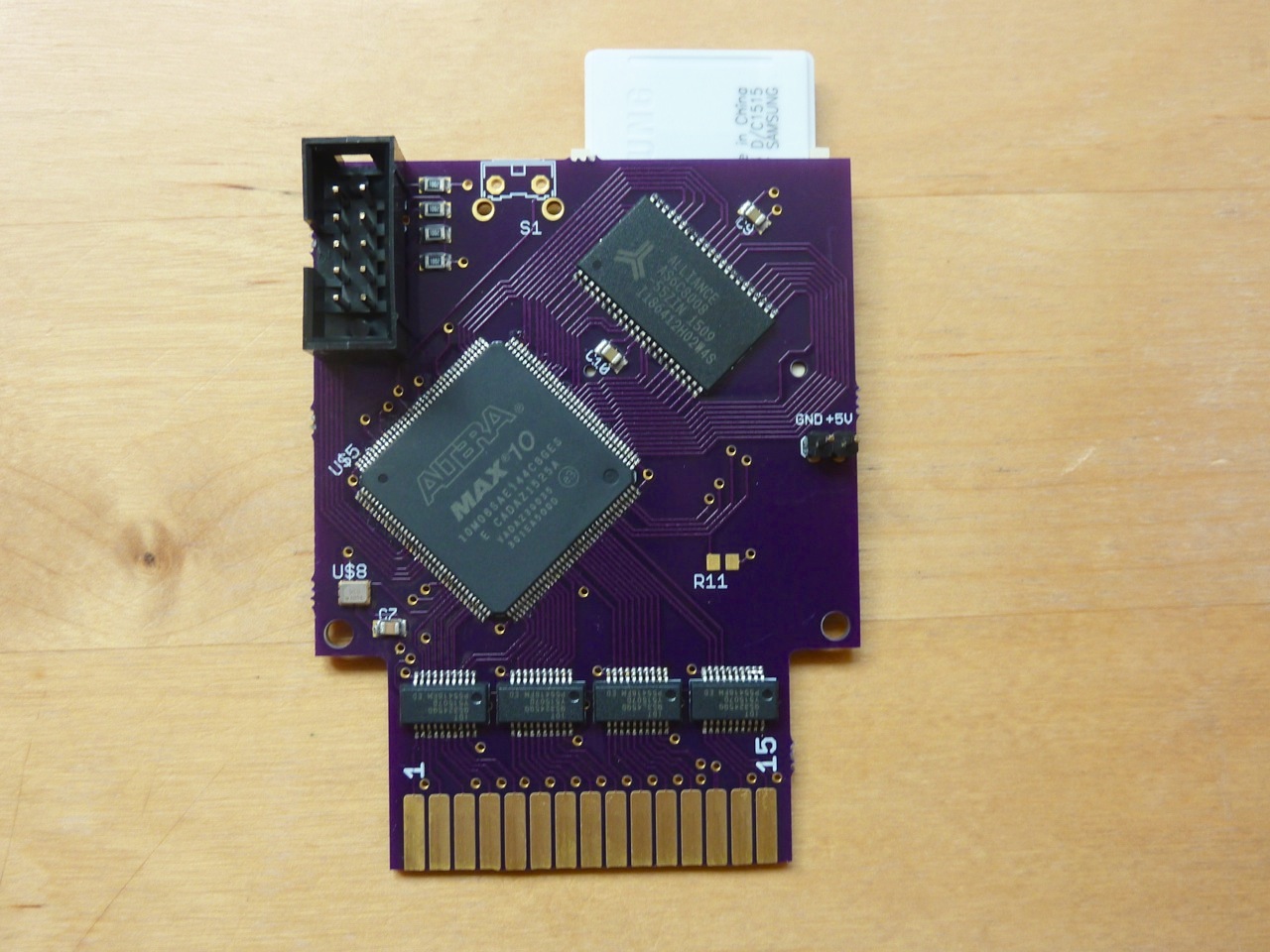
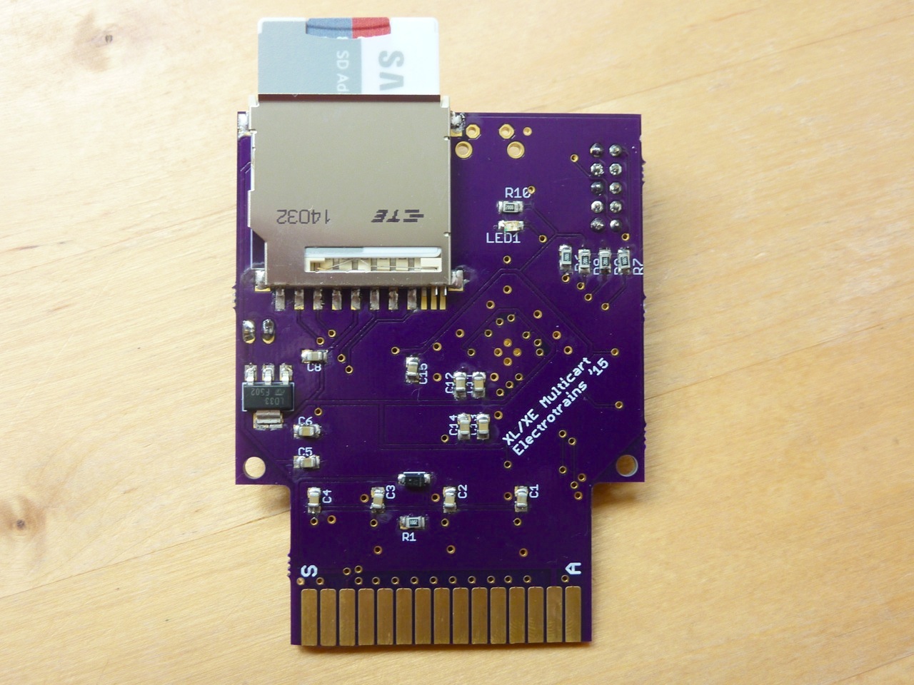
Although the schematic, board file and assembled images above are probably sufficient by themselves for a determined person to complete the board, here is the method I'm using to assemble the boards.
You will need:
Solder paste (I used standard chipquik unleaded) syringe
Some way of reflowing the board (e.g. cheap toaster oven)
Solder paste stencil for the fpga side (optional, but recommended - see below)
Tweezers (or a better tool) for placing the components
Soldering iron
Flux and braid to fix any bridged pins (you may not need if you use a stencil)
USB Blaster to program the fpga
Blu-tac I find useful for keeping things steady
You can either apply solder paste by hand (using a syringe) or using a stencil. Having done it both ways, I'd say the ten pounds I spent on a stencil was the best money I've ever spent! You can get a stencil made cheaply from a variety of places. I'd recommend either oshstencils (USA) or smtstencil.co.uk (UK). The paste layer was not correct on the original board, but was corrected in the revised version.
Apply the solder paste to the fpga side of the board, making sure you don't forget the ground pad. The revised board removes R11 (a pullup resistor on the SD card line) which is not required (since SD cards have an internal pull-up on CS).
Then populate the components, with reference to the marks on the board and the images above. Bake the board in an over until the paste melts (you'll see it shine), leave it for about 30s-1min, then open the oven door and let it cool.
Apply solder paste to the other side of the board (leaving the SD card which is hand soldered). There is less need for a stencil for this side of the board, a syringe is fine. Populate (make sure you get the polarity of the LED and diode correct) and bake again.
Before you do any hand soldering, check for bridged pins on the ICs. Some pins are bridged on the PCB - thats ok. Any others, use braid, flux and soldering iron to remove.
Next you will need to hand solder the jtag box header (slot facing outwards), and 2x1 male header.
Now is a good time to check for shorts - (1) between the +5V and GND pins of the male header, (2) between +3.3v and GND on the regulator, and (3) between VCC and GND on the IDT quickswitches. If you find a short then STOP and fix it. There will be a bridge somewhere. Refer to the eagle files to help identify the location.
Once that's done, you should be able to power up the board, plug in a USB blaster and program the chip from Quartus (use the pof file - this permanently programs the chip). If successful you should see the LED on the board blinking.
Finally, hand solder the SD card slot and reset button to the board. You're done!
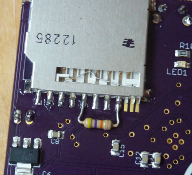
Someone who has built this project got in touch to report that some SD cards fail to be recognised. It appears that a 10k-100k pullup is required on the SD card DO (pin 7), or some cards will fail to initialise. I haven't come across this in the 10 different SD cards I've tested, but if you do have problems then you can fix it by adding a 47k pull-up resistor as shown in the photo below.
Note (1-Mar-16) - I have now uploaded a revised version of the board (v3) which adds this resistor to the PCB (labelled R11).
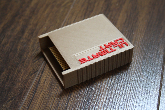
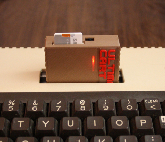
I have added STL files (and the source files) so you can use a 3d printer to make a nice cartridge shell for your PCB.
- Design, PCB & FPGA firmware by Robin Edwards (electrotrains at atariage)
- Atari boot menu & XEX loader by Jonathan Halliday (flashjazzcat at atariage)
- Debugging - Matthias Reichl (HiassofT at atariage)
- Help, suggestions and FAT32 LFN code from Mark Watson (foft at atariage)
