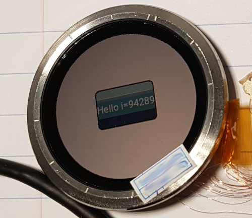
Bit-banging LCD display driver in Python for the Garmin Vivosmart 3 LCD. This is a proof-of-concept for the pyboard v1.1 which has an STM32 without FSMC. Hence, it uses bit-banging to drive the display.
In fact, despite being written for Micropython, the driver itself is mostly in ARM assembly. See lcd_v3.py for details.
- Wire up the LCD to the pyboard v1.1 I/O pins as shown in
lcd_v3.py. - Compile micropython with littlevgl bindings: lv_micropython. Ideally, freeze
lcd_v3.pyinto micropython to save RAM usage (see below). - Flash the pyboard with the newly built micropython using
dfu-util. - Place the files
lv_v3.py,boot.py,main.pyon the pyboard attached as a USB disk.
Freeze the bit-banging driver into micropython to reduce the RAM usage:
- copy
lcd_v3.pytoports/stm32/modules/lcd_v3.pyin thelv_micropythonfolder - in
ports/stm32/boards/manifest.py, add:freeze('$(MPY_DIR)/ports/stm32/modules', 'lcd_v3.py')
or look up usage of FROZEN_DIR make variable.
For the pyboard v1.1, I then built micropython in lv_micropython (github) using:
make -C ports/stm32 LV_CFLAGS="-DLV_COLOR_DEPTH=8" BOARD=PYBV11 all
Then I flashed the board, bridging BOOT0 to 3V3 with a jumper, resetting the board and using:
dfu-util --alt 0 -D ports/stm32/build-PYBV11/firmware.dfu
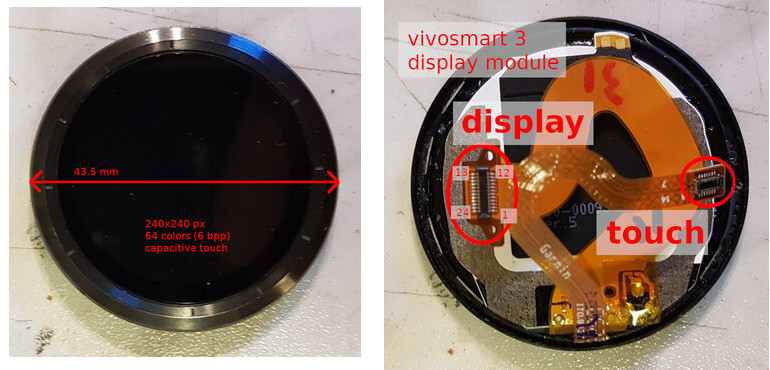
For a custom smartwatch device, I needed a round LCD display with a touchscreen. Shopping around a little bit on AliExpress and Banggood, the options seemed limited to rectangular displays with an aspect ratio that would leave most of the watch's front unused - and no touch screen. Then, I stumbled upon a replacement display module for the Garmin Vivosmart 3. Needless to say, this module came without a datasheet.
Most of the inspiration for this project came from https://www.youtube.com/watch?v=7TedIzmguP0 - if you are serious about reverse-engineering a display interface, you should definitely watch this.
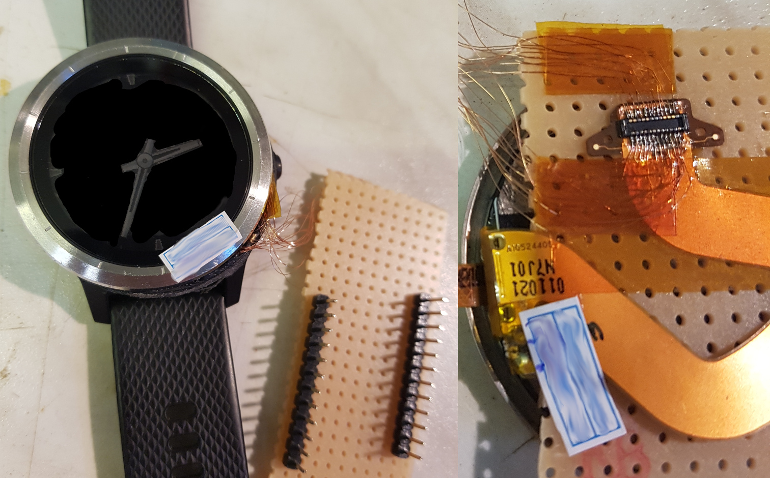
To measure how the display is controlled, I purchased a used Garmin Vivosmart 3 smartwatch from ebay. I opened it using some hot air (the display module is glued on), then attached 0.15 mm wires to the display data connector. I had some fun soldering those! For future reference, the connector is 0.4 mm pitched, and the Hirose receptacle BM20B(0.6)-24DS-0.4V(53) almost fits it (but it is slightly too narrow). It would be possible to order a header/receptacle pair, and replace the header on the display's FPC...
First, I measured the voltage on the pins using a DMM, and then moved on to an oscilloscope to check for higher-frequency components.
There is a Garmin app (Connect IQ) that allows a paired smartphone to upload watch face images. I uploaded some line patterns to the watch, and could verify the pattern changing on the data pins.
| Label | Pin | Pin | Label |
|---|---|---|---|
| 1.04 V floating | 12 | 13 | 3.2 V |
| 1.04 V floating | 11 | 14 | 0.23 V floating |
| 200 µs end pulse | 10 | 15 | 5 V |
| 100 µs period rect: row | 9 | 16 | 100 µs begin pulse |
| chip select | 8 | 17 | 50 µs period rect: 40% duty cycle (not critical; maybe some PWM) |
| 60 Hz rect | 7 | 18 | 60 Hz rect, opposite phase to pin 7 |
| GND | 6 | 19 | 3.2 V |
| 1.2 MHz clock | 5 | 20 | hsync_start (hairpin impulses every 50 µs at the row start) |
| data (red on odd pixels) | 4 | 21 | data (red on even pixels) |
| data (green on odd pixels) | 3 | 22 | data (green on even pixels) |
| data (blue on odd pixels) | 2 | 23 | data (blue on even pixels) |
| 60 Hz rect, in phase with pin 18 | 1 | 24 | hsync_end (hairpin impulses every 50 µs at the row end) |
Screen resolution is 240x240 pixels. Data is transferred both on rising and falling clock edges. The transfer pattern is blocks of 4 horizontal pixels each. For every row, there are two transfers, first the LSB and then the MSB bits. For complete details, see the comments in lcd_v3.py, excerpted here:
# # Transfer pattern
#
# 4 horizontal pixels  x  2 vertical pixels block:
#
# ```
# {[P_hf T_i] [P_lf T_i] [P_hr T_i] [P_lr T_i]}
# {[P_hf T_o] [P_lf T_o] [P_hr T_o] [P_lr T_o]}
#
# T_i is transfer slots [1,0]
# T_o is transfer slots [3,2]
#
# P_ab
# a: h for pins 21,22,23, l for pins 2,3,4
# b: f for falling edge, r for rising edge
# ```
#
# Each transfer_frame transfers one row's (LSB or MSB) for the entire screen.
# Each full clock cycle, 4 pixels in {} are transmitted.
#
# After all T_i slots (2 x 61 clks in transfer_frame) of even row,
# the odd row is transmitted with T_o slots (again 2 x 61 clks in transfer_frame).
Using a digital storage oscilloscope, I recorded the data pins as the display is updated. Then, I transferred those recordings to my computer, and started decoding the data.
- I uploaded test patterns to the watch screen using Garmin Connect IQ and measured signals until I had the pixel layout on the wire. During this, I wrote a Python script decoding the recorded oscilloscope data.
- Later, I wrote a second Python script generating the pixel layout from an image buffer, and verified that I could decode it with the first script.
- Finally, I re-wrote the second Python script for Micropython.


