I got busy and development has halted for a while. I plan to continue and complete this repo and would also welcome any contribution from others as well. Stay tuned for the bash script to install the tools for analog design flow(xschem+sky130pdk+ngspice+magic+netgen), that is in priority for now. Also special thanks to Rajdeep for mentioning this repository in his videos, now I have a responsibility to manage it better which I am really excited for!!.
This project has only one motive; that is to experiment with working of an inverter and understanding all the parameters involved with it. The design will utilise the models that are present under the skywater 130nm pdk and various open source tools such as, Xschem, NGSPICE, MAGIC, Netgen, etc.
The whole process starts with analysis of NMOS and PMOS devices, specifically the 1.8v standard models available inside the pdk to determine a common working W/L ratio and also the gm, ron and similar values. After this we start with the design of a CMOS inverter that includes schematic, measurement of various parameters like delays, noise margin, risetime, falltime, etc. This part would also act as a case study on SPICE where we use it's programming capabilities to better our abilities in measurements of aforementioned parameters. Then we will engage in the design a layout for our inverter in magic layout editor. Here, we will also explore the different layers available to the user and how we utilise them in a design and what it translates to in terms of a mask. Lastly, we compare the two netlists, that is the schematic and the layout one, which is popularly referred to as LVS. If everything is hunky-dory, this project would then conclude.
I will try to keep updating it as often as possible, as this first project is a primary resource for me to practice analog design, with the open source toolchain and definitely to keep a documentation that is easily understandable by anyone who later tries to practice it the same way.
Let's get right into it.
Section 1 has been referenced from VSDOPEN21_BGR Readme file Thanks Kunal!
For the design and simulation of our Inverter.
- Spice netlist simulation - Ngspice
- Layout Design and DRC - Magic
- LVS - Netgen
- Schematic Capture - Xschem
Make sure all the libraries that are necessary for all these below software are installed in your system. Also this would cost a lot of space as well so I suggest to get atleast 50GB of storage and atleast 8GB RAM.
I have created a bash script to do that, use this file to install all the dependant libraries for the below software. I am in the process to create one script to install all the below, but that is for some other day.
Ngspice is the open source spice simulator for electric and electronic circuits. Ngspice is an open project, there is no closed group of developers.
Ngspice Reference Manual: Complete reference manual.
Steps to install Ngspice -
Don't use the version that comes with linux distribution, since it is dated and sometimes misses crucial updates
Follow this video for just the ngspice installation. DO NOT use this video to install xschem and skywater-pdk.
The above video should be fine but if it does not work for you, Follow the instructions given inside the INSTALL and README file that comes inside the git clone of the repository of ngspice
Magic is a VLSI layout tool.
Steps to install Magic - Follow the instructions on the Opencircuitdesign Install section. I would suggest to use a couple options for the configuration file.
Netgen is a tool for comparing netlists, a process known as LVS, which stands for "Layout vs. Schematic". This is an important step in the integrated circuit design flow, ensuring that the geometry that has been laid out matches the expected circuit.
Steps to install Netgen - Open the terminal and type the following to insatll Netgen.
$  git clone git://opencircuitdesign.com/netgen
$  cd netgen
$  ./configure
$  sudo make
$  sudo make install
Xschem is a schematic capture program that allows to interactively enter an electronic circuit using a graphical and easy to use interface. When the schematic has been created a circuit netlist can be generated for simulation.
Steps to install Xschem Follow the instructions given here.
A process design kit (PDK) is a set of files used within the semiconductor industry to model a fabrication process for the design tools used to design an integrated circuit. The PDK is created by the foundry defining a certain technology variation for their processes. It is then passed to their customers to use in the design process.
The PDK we are going to use for this BGR is Google Skywater-130 (130 nm) PDK.

Steps to download PDK - Open the terminal and type the following to download sky130 PDK.
$  git clone https://github.com/RTimothyEdwards/open_pdks.git
$  cd open_pdks
$  ./configure [options]
$  make
$  [sudo] make install
You should follow the instructions given at this link
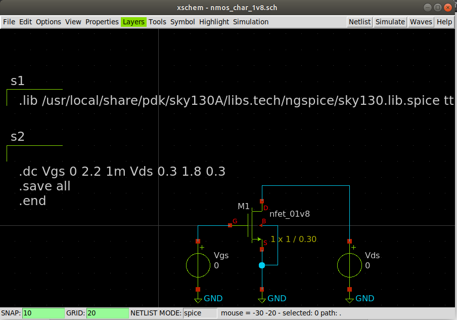
In this section I start with our analysis of MOSFET models present in sky130 pdk. I would be using the 1.8v transistor models, but you can definitely use and experiment with other ones present there. below is the schematic I created in Xschem.
highly recommended to check out the tutorials of xschem here and ngspice here
The components used are:
nfet_01v8.sym - from xschem_sky130 library
vsource.sym - from xschem devices library
code_shown.sym - from xschem devices library
I used the above to plot the basic characteristic plots for an NMOS Transistor, That is Ids vs Vds and Ids vs Vgs. To do that, just save the above circuit with the above mentioned specifications and component placement. After this just hit Netlist then Simulate. ngspice would pop up and start doing the simulation based calculations. It will take time as all the libraries need to be called and attached to the simulation spice engine. Once that is done, you need to write a couple commands in the ngspice terminal:
display - This would display all the vectors available for plotting and printing.
setplot - This would list all the set of plots available for this simulation.
after this choose a plot by typing '''setplot <plot_name>'''. for example '''setplot tran1'''
plot - to choose the vector to plot.
example : plot -vds#branch
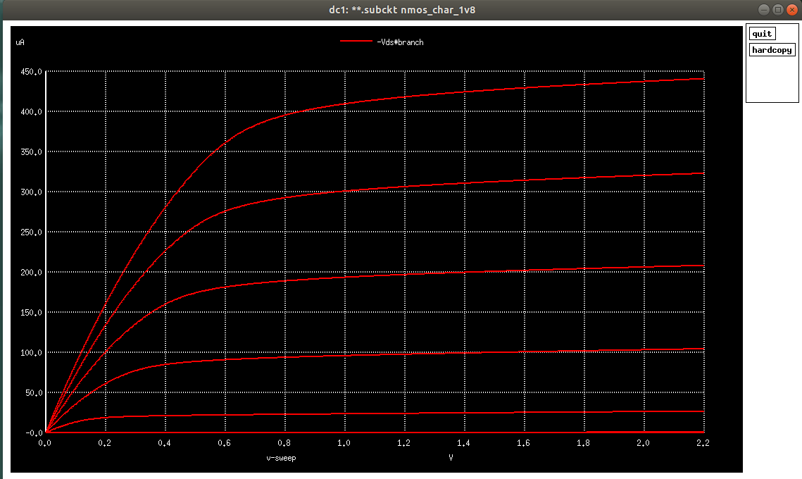
Then you must see the plot below you, if you did a DC sweep on the VGS source for different values of VDS:
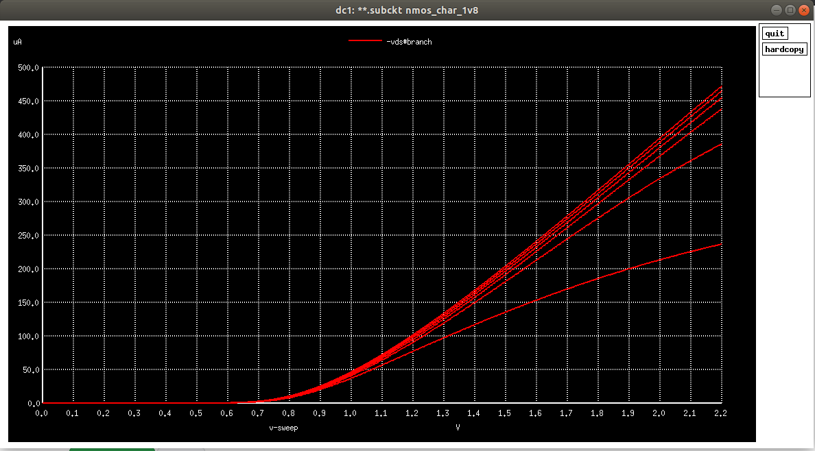
This definitely shows us that the threshold value is between 600mV to 700mV and I think I will be using 650mV for my future calculations.
Similarly, when I sweep VDS source for different values of VGS, I get the below plot:
Now the above two definitely looks like what the characteristics curves should, but now we need to choose a particular curve that we would do further analysis on.
I also did plot gm and go(or ro) values for the above mosfet. This would be crucial as we can obtain a lot of parameters from these values. Both of these below are for the general dc sweep we did above.
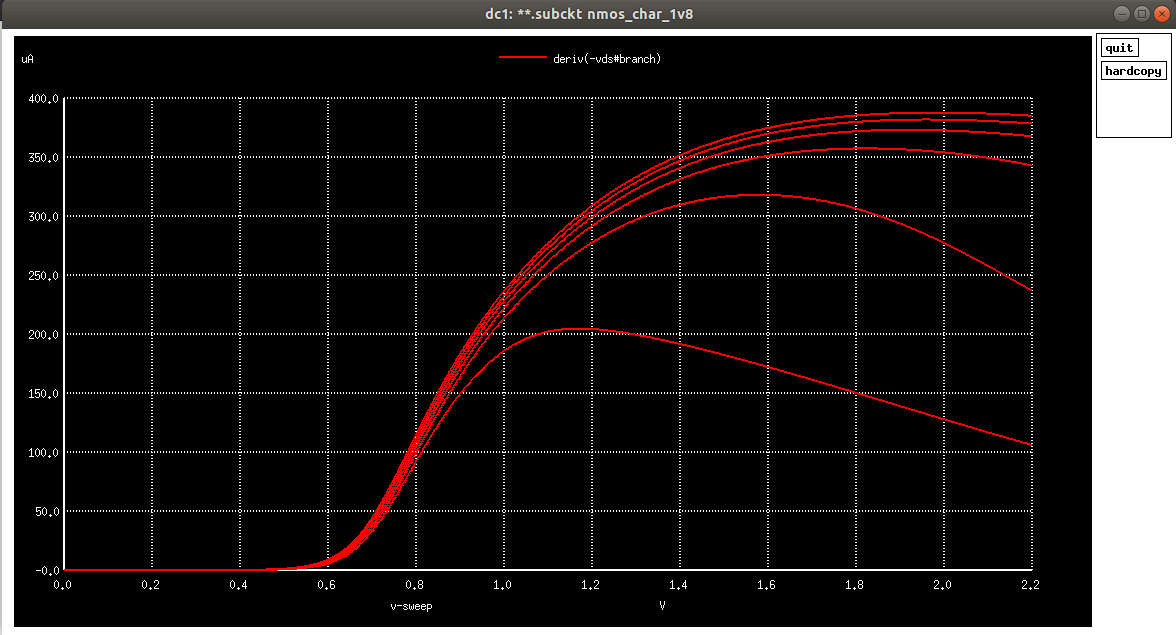
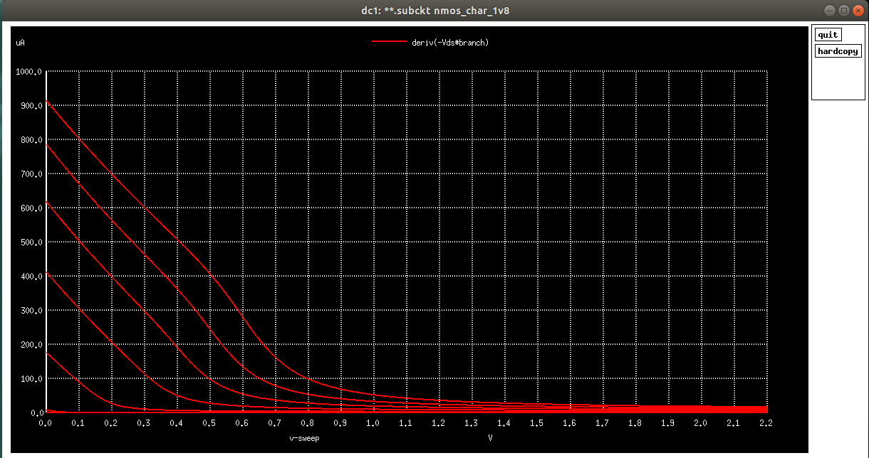
Since I am making an inverter, let's choose the highest value avialable for the Vds, that is 1.8V. So to do that, we just change the value of Vds source to 1.8 and then hit netlist, then simulate to simulate the circuit.
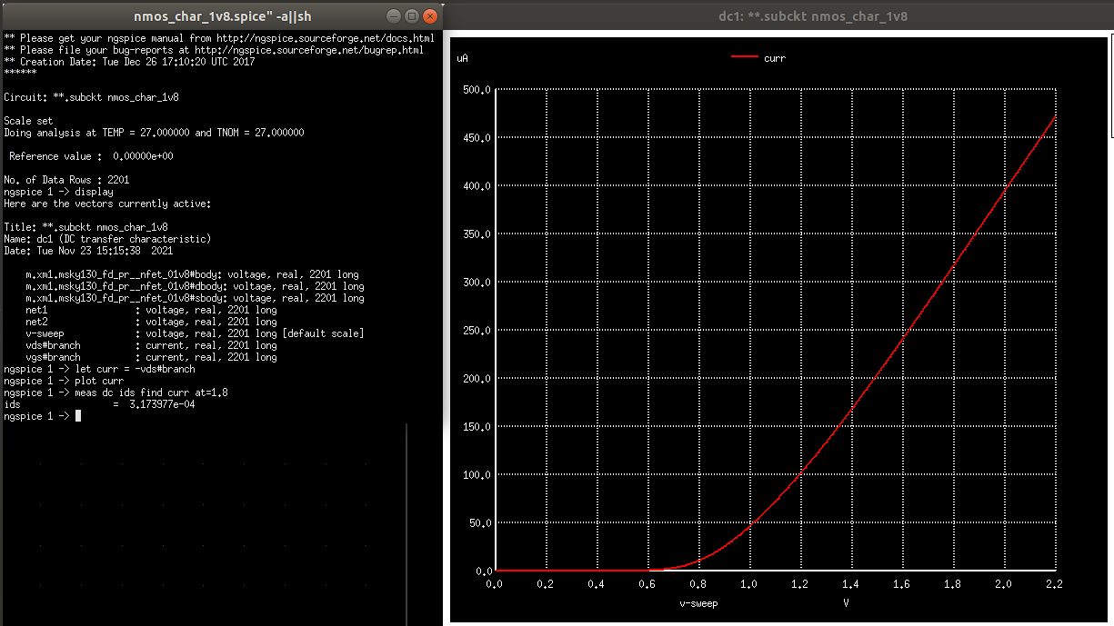
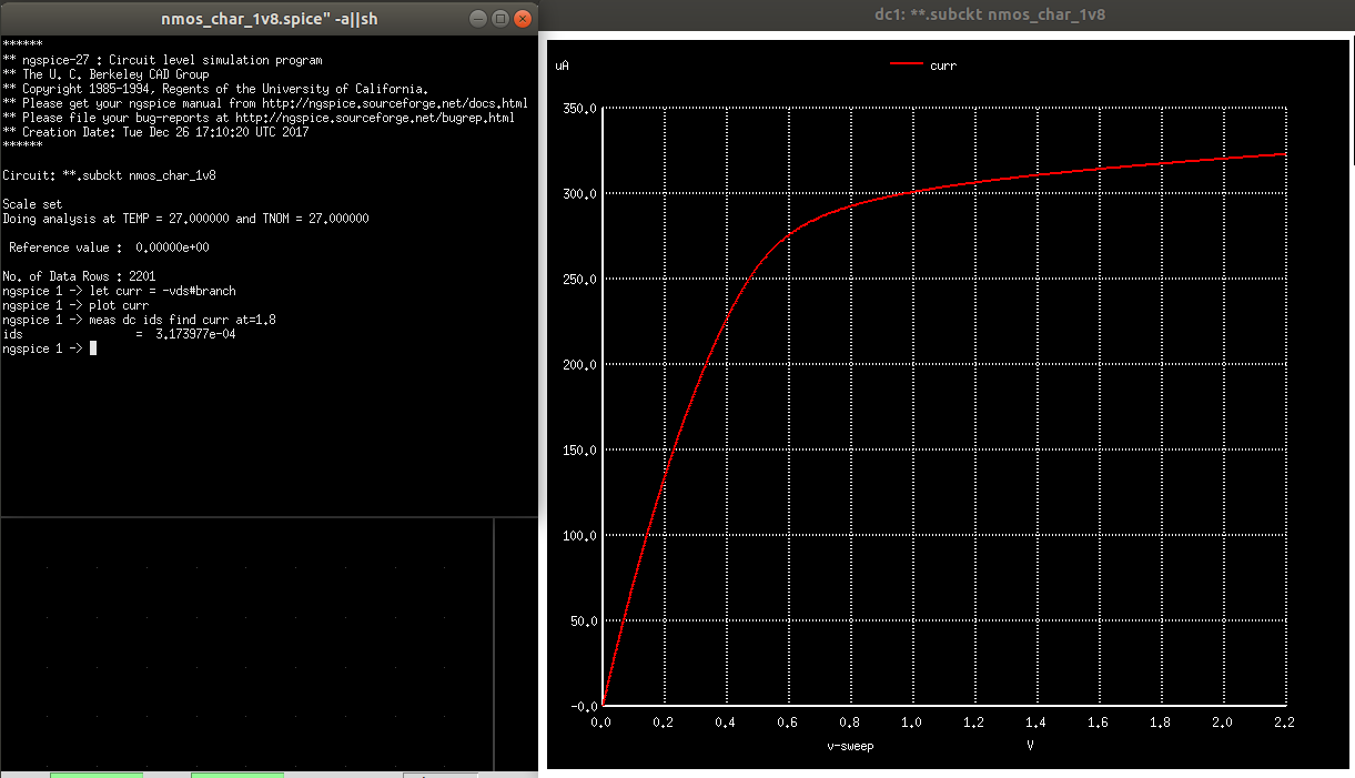
This above plot also tells us the value of current at this value of Vgs which is around 320uA. Next step is to calculate the Gm, that is the transconductance parameter. To do that we simple type the commands as shown in the console in the left hand side. The deriv() function takes the derivative with respect to the independent variable present at the current simulation. From the definition of Gm we are aware that it is dIds/dVds. Hence, I did the same to plot the Gm of this nfet. After this I measured the value at 1.8V.
Information on how to use the meas command can be found at ngspice manual !
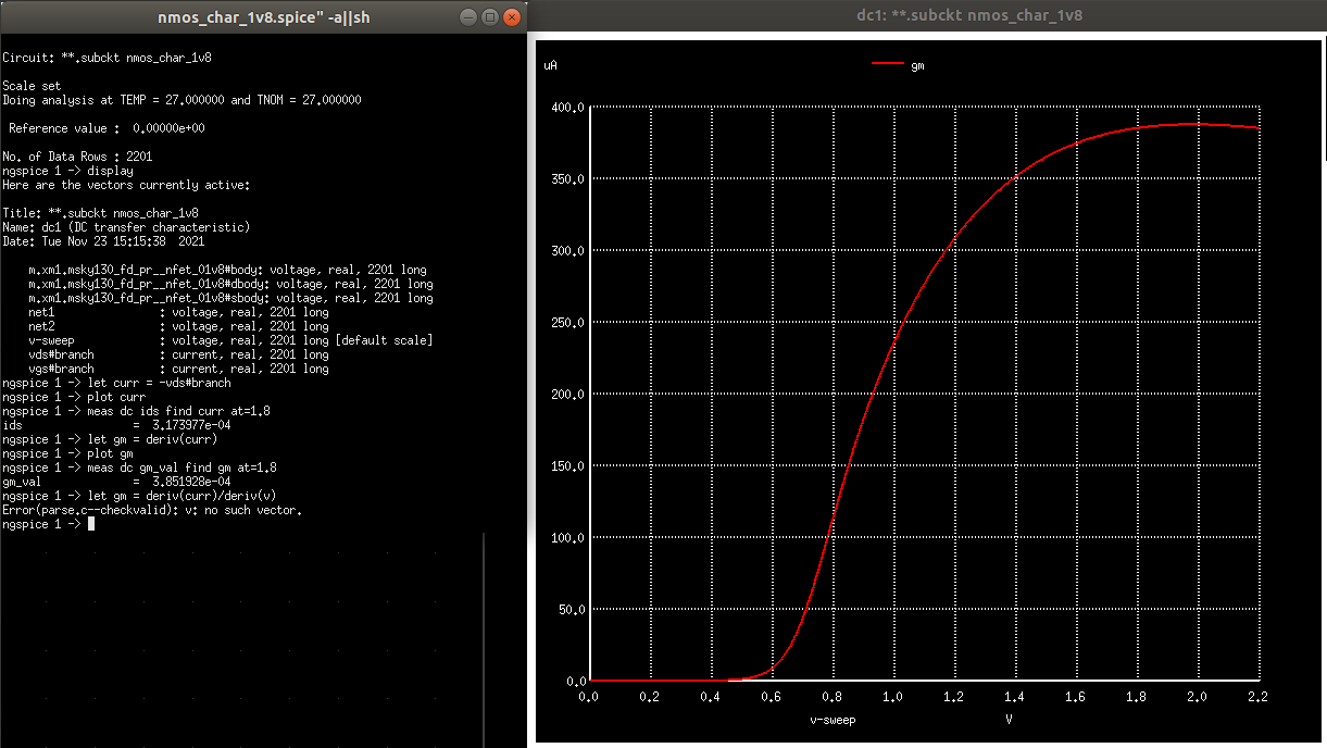
Similaraly I did the same for Ids vs Vds and also used that to find rds
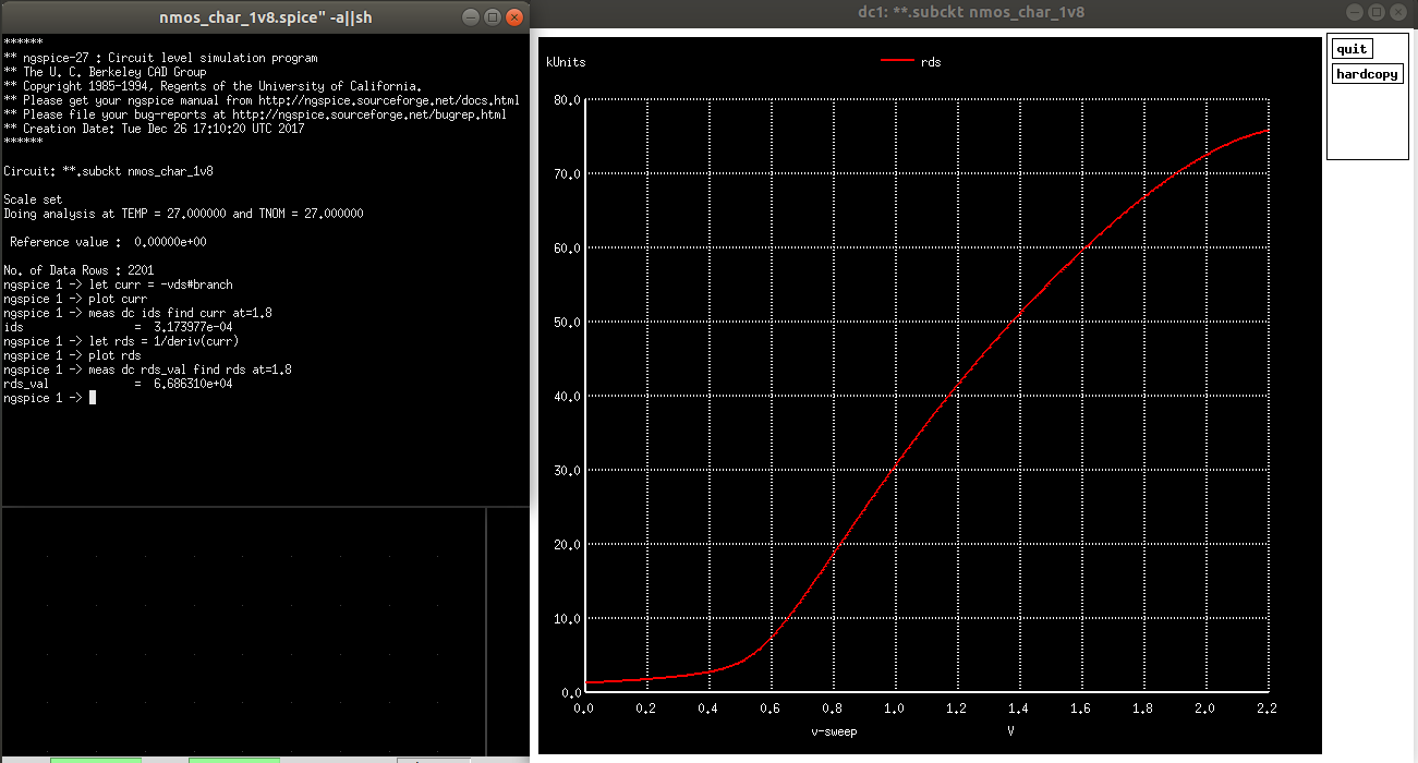
Hence, we now have all our important values we needed. Same can be done for a PMOS. Motive is same, but expecially to extract the value of Aspect ratio for which the current is the same in both NMOS and PMOS. I have done some experimentation and found that at W/L of PMOS = 4 * (Aspect ratio of NMOS), the current value is pretty close. So, we found the NMOS had a current of 317 microamps while PMOS has the current of 322 microamps (both at |Vgs| = 1.8V). SO like 5 microamps apart. (NOT BAD!!)
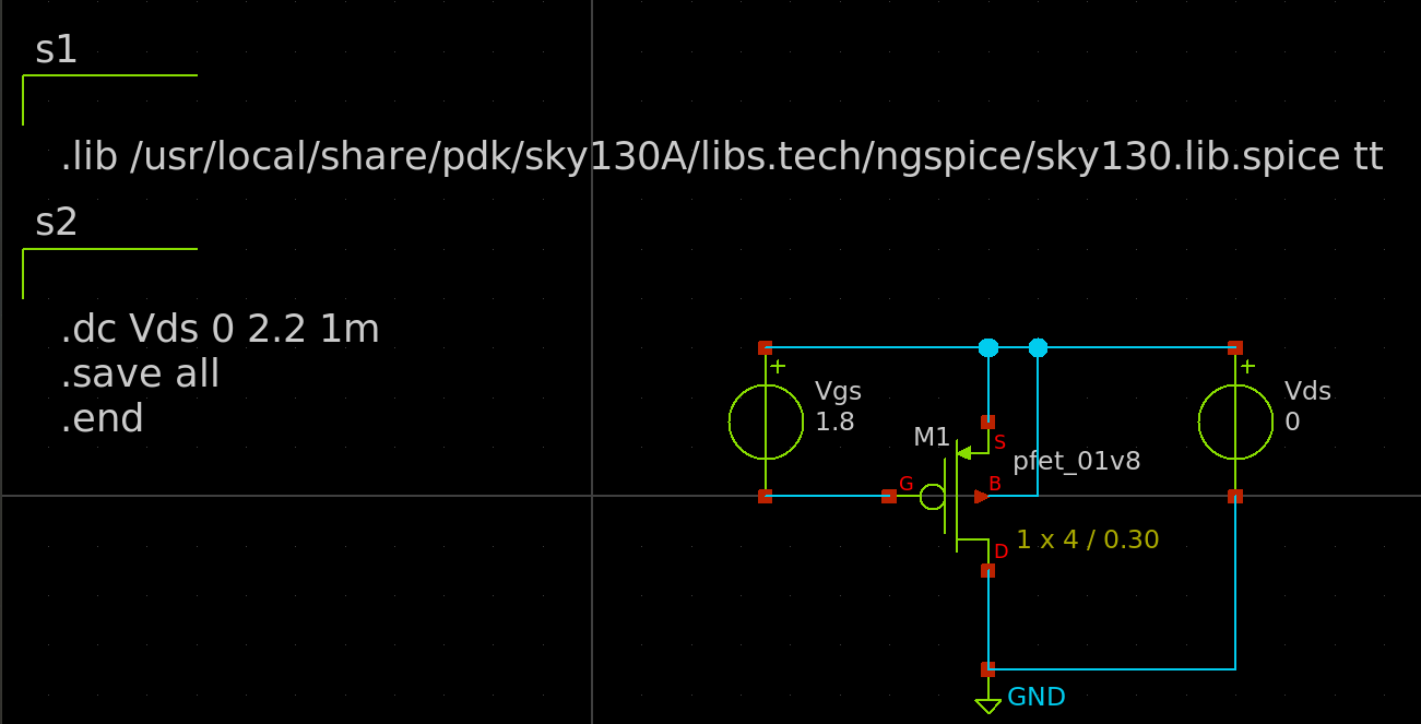
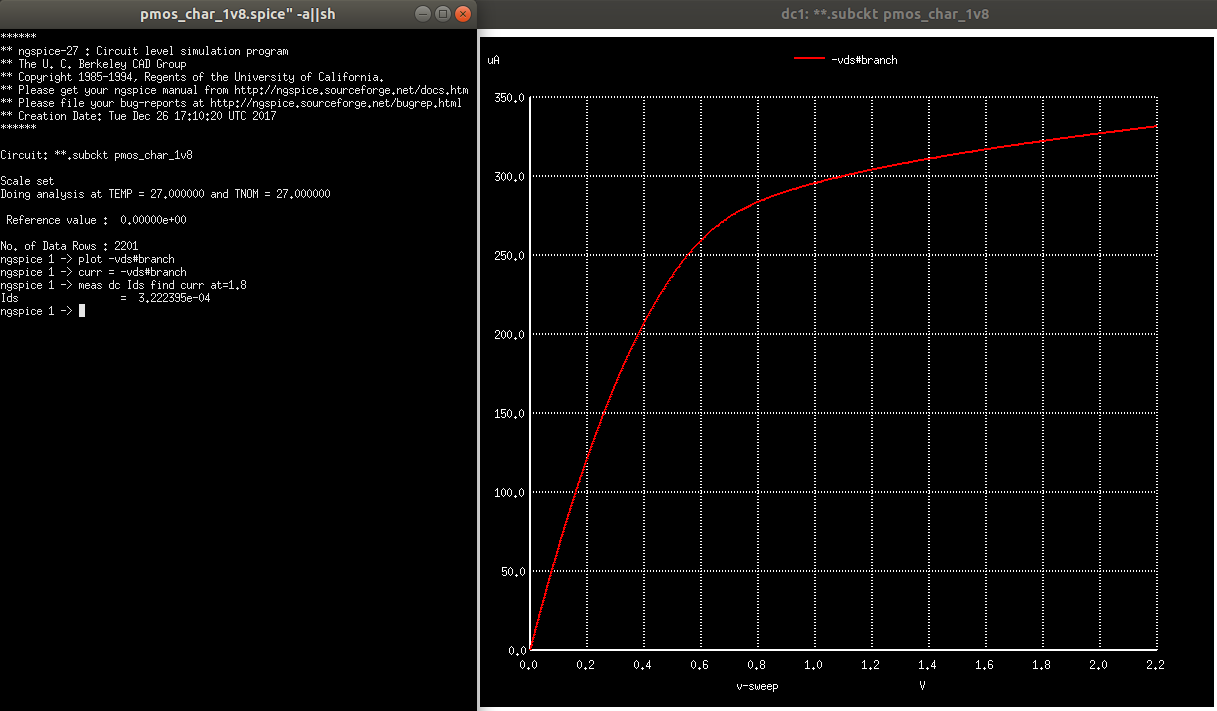
The last one might be the most important one for an Inverter design
What does the above mean? Look at the graph below,
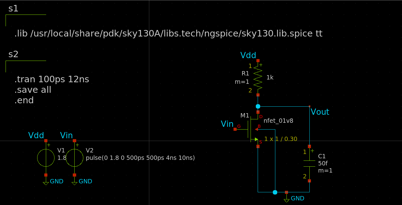
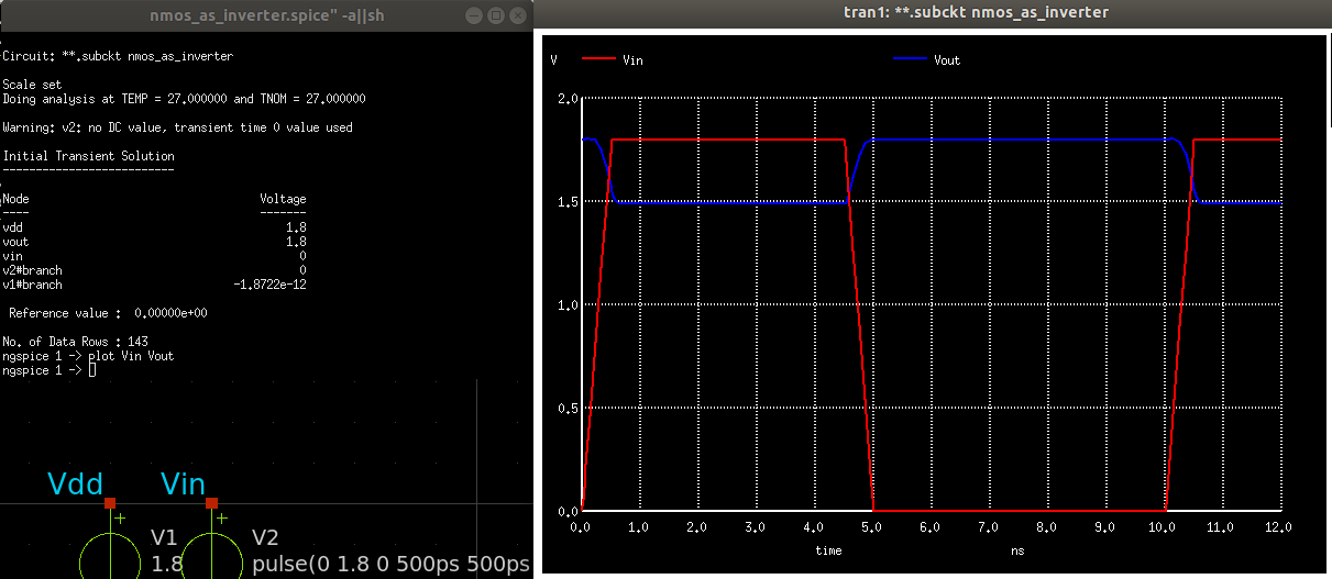
You can see that, when a square wave is applied to the input of NMOS, when it is LOW(0V), the output goes to HIGH(1.8V). But when the input is HIGH(1.8V), the output goes to a value that is much larger than 0V. This is due to the fact that when Vgs is 1.8V, the NMOS is in linear region. This is where the MOSFET acts as a voltage controlled resistor. At this point, the output is connected to a Voltage Divider Configuration. That is the output takes the value which is defined by the voltage across the resistance of the mosfet. Hence, NMOS is able to transmit STRONG 0, but not a STRONG 1. So NMOS is Strong 0 but a Weak 1
Again, some plots will clear the idea
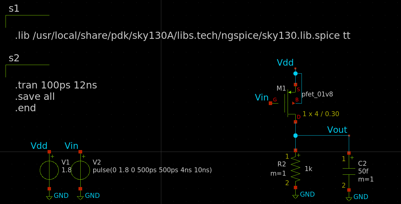
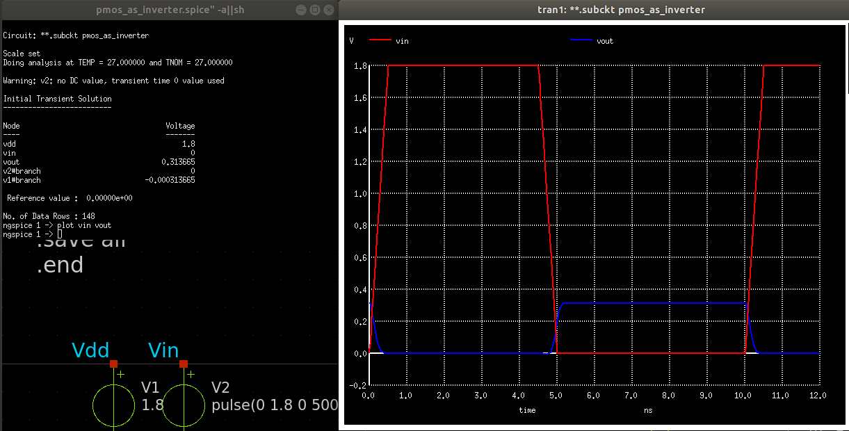
The reasoning is the same as the previous section
Hence, neither NMOS nor PMOS would make a great inverter on their own. So a plethora of configurations were taken into account, but at the last, only one stands as the most popular format of circuit design using mosfets. It is referred to as a CMOS configuration
An interesting obseration was made in the previous section, where we realised that neither NMOS nor PMOS can be used for design that can produce either values, HIGH and LOW. But another thing that is worth notice is how they complement each other. This is what gave rise to an idea of attaching them together. Since, PMOS is a Strong 1, we put it between VDD and Vout and NMOS being a STRONG 0, it is placed between Vout and GND. This way, either can act as a load to the other transistor, since both are never ON together (Are they?). The configuration looks like what we have below. This is referred to as Complimentary Metal Oxide Semiconductor(CMOS) Configuration and it also represents the simplest circuit known as the CMOS Inverter.

CMOS Circuits generally consists of a network split into two parts, Upper one referred to as a pull up network and the lower half as a pull down network. The former consists of P-channel MOSFETs and later N-Channel MOSFETs. Reason is simple. As one transistor is one, another is off. This eliminates the issue of an resistive path to the ground and hence, no voltage division occurs(At least not a significant one). This way, one can easily achieve a Strong High and a Strong LOW from the same network. PULL UP is what offers a low resistance path to the VDD and PULL DOWN is what offers a low resistance path the GND.
Before, I start with the CMOS inverter, I believe it is worth mentioning what an Inverter is. Inverter is something that inverts. In electronics it is very popularly explained as something that performs the NOT logic, that is complements the input. So a HIGH(1.8V) becomes LOW(0V) and vice versa. Ideally, the output follows the input and there is no delay or propogation issues of the circuit. But in reality, an inverter can be a real piece of work. It can have serveral isseus like how fast can it react to the changes in the input, how much load can it tolerate before it's output breaks and so many more including noise, bandwidth, etc.
All these parameters are what will always plague any analog design or design with transistor in general. Hence, with inverter many like to explore them all. So it justifies why Inverter is referred to as Hello World! of transistor level design. Atleast, I say that 🤣. So in this section that took me aeons to reach to, we finally start with all the important analysis and parameters to be evaluated for an Inverter. I first start with a schematic diagram, then I evaluate all the parameters, that is, measuring them, experimentin with them and reaching a conclusive value and Finally reach a schematic circuit that is capable of things we lay down at the beginning.
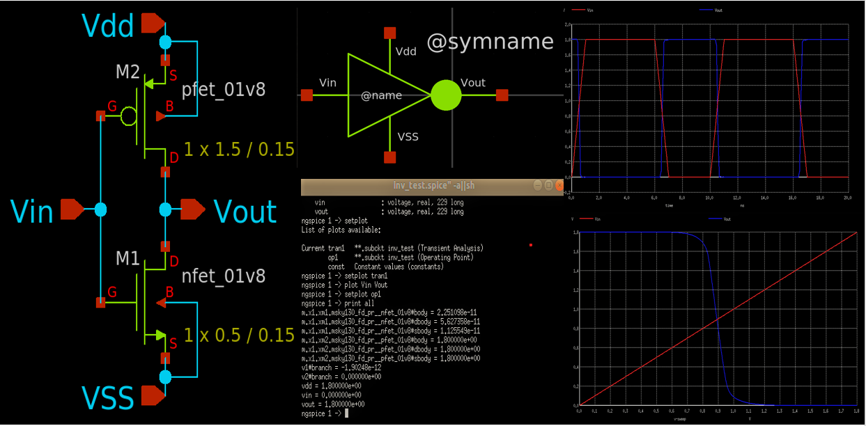
So I designed a Schematic of the Inverter, where the whole thing is based on what we determined earlier. I have chosen (W/L) of PMOS = 4 times (W/L) of NMOS and (W/L) of NMOS is 1/0.30 in microns. I also designed a symbol of it, so that we can utilise that for further schematic creation.
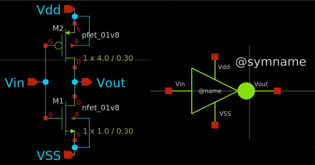
A lot of calculations will now start from this point. Similar to how we analysed for MOSFETs individually. Also from now on, (W/L) would be mentioned as S or Aspect Ratio Simply. We would use the following testbecnch for future analysis.(Transient and DC)
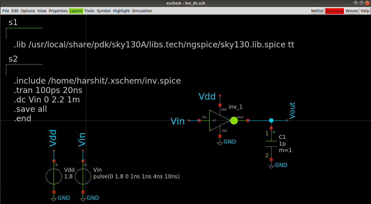
DC analysis would be used to plot a Voltage Transfer Characteristics (VTC) curve for the circuit. It will sweep the value of Vin from high to low to determine the working of circuit with respect to different voltage levels in the input. The following plot is observed when simulated :
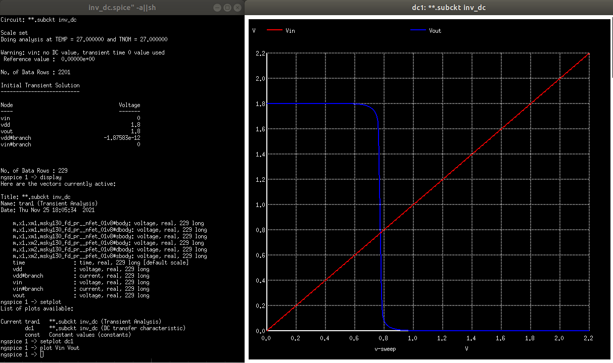
A voltage transfer characteristics paints a plot that shows the behavior of a device when it's input is changed(full swing). It shows what happens to the output as input changes. In our case, for an inverter we can see a plot that is like a square wave(non ideal), that changes it's nature around 0.75 volts of input. So one can say that there are like 3 regions in the VTC curve, the portion where output is high, the place of transistion and the one where the output goes low. But actually there are five regions of operation and they are based on the working of inverter constituents, that is the NMOS and the PMOS transistors with respect to the change in the input potential.

One can solve for them using the equations for individual transistors. Now it is time to talk about the important parameters of this device that are based off it's VTC curve.
- VOH - Maximum output voltage when it is logic '1'.
- VOL - Minimun output voltage when it is logic '0'.
- VIH - Maximum input voltage that can be interpreted as logic '0'.
- VIL - Minimum input voltage that can be interpreted as logic '1'.
- Vth - Inverter Threshold voltage
Above five are critical for an Inverter and can be seen on the VTC curve of an inverter. One thing to point out now would be,
Vth should be at a value of VDD/2 for maximum noise margins
And I tried to do that with our calculated inverter values at l=300nm but guess what! It did not work at all. I know there has to be a reason for it, which I will try to investigate further, but as of now, I changed the device parameters to get Vth close to the values Vdd/2. Now our NMOS has S = 1.05/0.15 and PMOS has S = 2.1/0.15. Below is it's simulation result using the same testbench.
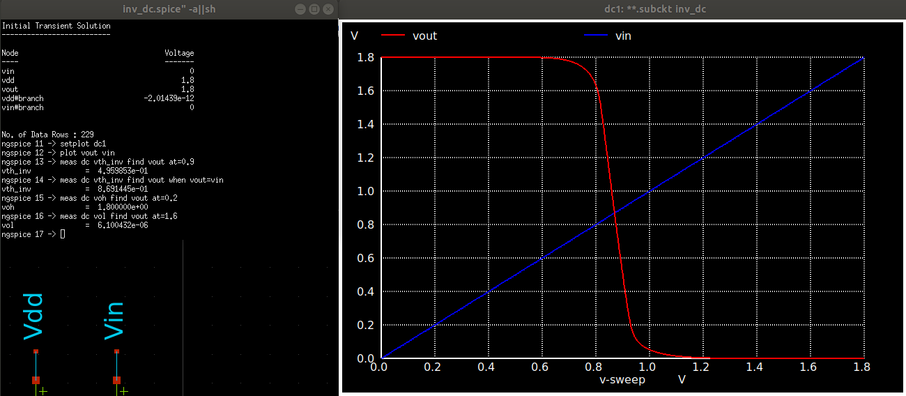
VOH and VOL are easy to determine as they are your aboslute values. In our case it is 1.8V and 0V respectively. For Vih and Vil, we have another method. At Vin = VIH, NMOS is in Saturation region and PMOS in Linear; while when Vin = VIL, NMOS is in Linear and PMOS in Saturation. Another interesting thing about these points is that, these are the points on the curve, when the magnitude of slope = 1. So we can use measure commands to find them on the plot. In the plot shown below, look at the points that are at the intersection of the vout curve and the blue vertical line. These are our VIH and VIL.
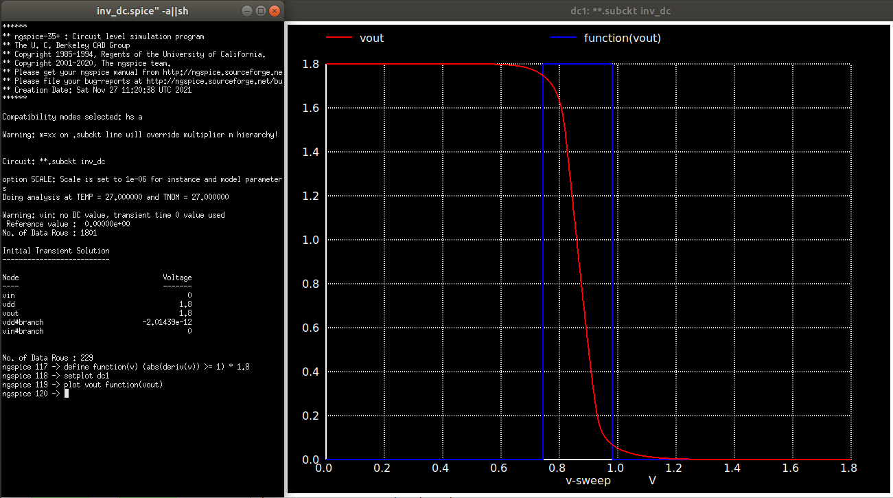
And to calculate them, we use .meas statement with apt instructions. The result is down below.
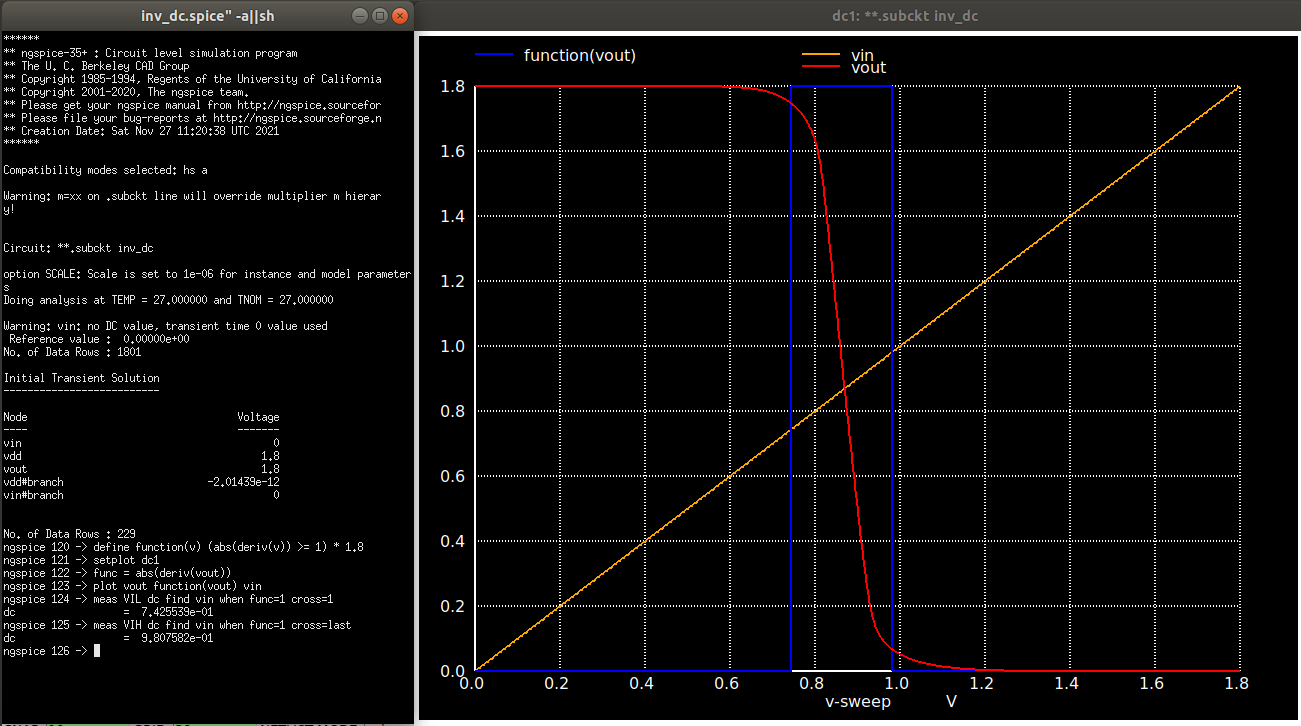
Look at the commands used carefully. The first lines declares a function, that I have used to see at what region is the derivative of Vout with respect to Vin greater than or equal to one. This has no significance other than visualizing what region is the one where transition occurs. After this I set the plot to dc1, which is the identifier for the first dc analysis done for the netlist. Then it was just plotting them all and using the measure statements to determine the values necessary.
Let's summarize the values obtained :
| Voltage | Value |
|---|---|
| Vth_inv | 0.87V |
| VOH | 1.8V |
| VOL | 0V |
| VIH | 0.98V |
| VIL | 0.74V |
Now all the basic defining characteristics of an inverter are done. So we can find a couple more things and then proceed towards the transient analysis. Next is Noise Margins. Noise margins are defined as the range of values for which the device can work noise free or with high resistance to noise. This is an important parameter for digital circuits, since they work with a set of specific values(2 for binary systems), so it becomes crucial to know what values of the voltages can it sustain for each value. This range is also referred to as Noise Immunity. There are two such values of Noise margins for a binary system:
NML(Noise Margin for Low) - VIL - VOL
NMH(Noise Margin for HIGH) - VOH - VIH
So for our calculated values, the device would have, NML = 0.74V and NML = 0.82V.
Now, they aren't equal. But if we were to take some more effort to get the values of Vth closet to Vdd/2 (0.9V), then we can get NML = NMH. But for our case they are close enough. Then a last parameter that is crucial for any design is the power it consumes. The Power Dissipation of our inverter is given by P = Vout * Id, where Id is the drain current. I think I have not added a plot of the drain current yet. So let's do that below and calculate the power consumption of our inverter.
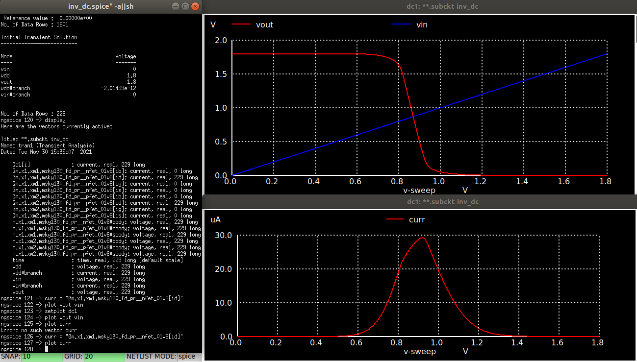
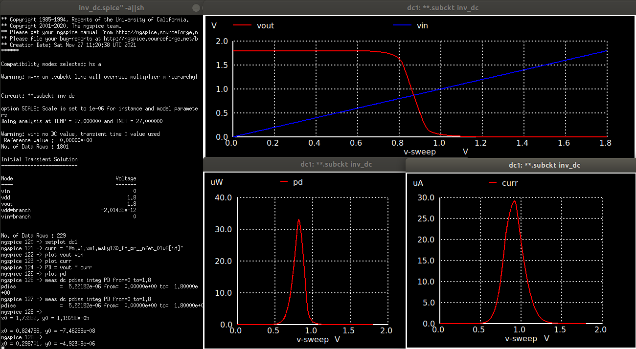
Hence, the total Power Dissipation = 5.55u Watts for our device. Also, notice how current only spikes up when the transistion occurs. This region is referred to as transition region and it's width is given by (VIH - VIL) = 0.24V. So there is almost 0 watts of power consumed!!! when the device is at VOH or VOL, that is power only consumed when switching between states.
Now, let's analyse the inverter with variations in it's design parameters, like Width(W), VDD and Cload. To write a parametric sweep, we have to write a script inside our netlist. Let's proceed.
(A) VDD supply variations
I have added the following script inside the spice netlist for out inv_testbench.
.control

let supply = 1.8
alter Vdd = supply
	let VDD_start = 0
	dowhile VDD_start < 6
	  dc Vin 0 1.8 1m
	  let supply = supply - 0.3
	  alter Vdd = supply
	  let VDD_start = VDD_start + 1
  end
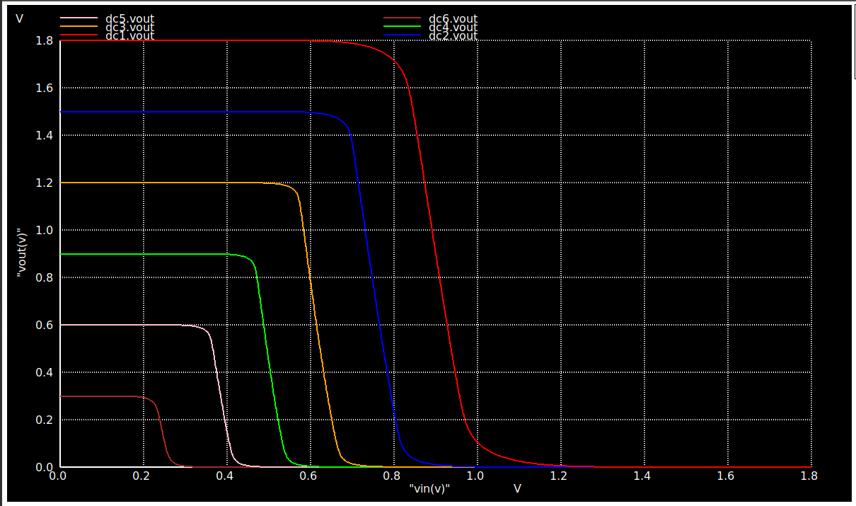
plot dc1.vout vs vin dc2.vout vs vin dc3.vout vs vin dc4.vout vs vin dc5.vout vs vin dc6.vout vs vin xlabel "Vin(V)" ylabel "Vout(V)" title "Inverter VTC with vdd variations"

.endc
The above control block would sweep vdd from 1.8V and 0.3V in steps of 0.3V, in ngspice and do dc analysis for all of them. The below is the plot for the this netlist
