Welcome to the first class on classical Computer Science! Beginning now, you will be studying the underpinnings of the programming lessons that you have practiced previously.
The first pair of sprints in this coursework are about your computer itself: computer architecture. Generic computers are just a large and careful collection of basic electronics components and wires connecting them. Computer architecture is the specific design of a computer.
We can't start our study of computers without a brief discussion of computer engineering. Know what the following words mean:
- Transistor
- Logic gate
- RS Flip Flop

Computers have grown radically in transistor density and clock speed, but the overall design of your computer has not changed tremendously since the 8086 in 1976 1. Modern computers utilized a fixed component architecture, where separate components can be upgraded, swapped, or redesigned for the next version with minimal impact on other components. It helps to visualize these components on a full size ATX form-factor motherboard:


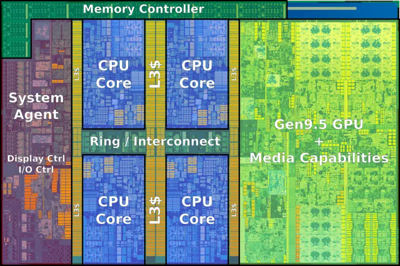

Amazing explanation of Kaby Lake CPU architecture
CPU, Clock(s), Program Counter, Instruction Register, Arithmetic Logic Unit, bus(es), RAM, Registers, Operations
-
CPU - a general purpose hardware component built with custom hardware to: read and write memory, perform arithmetic
-
Clock(s) - Special pieces of electronics hardware that cause a small voltage cycle at an insanely fast speed. Kaby Lake clocks: base, core, ring, IGP, eDRAM, Mem
-
Registers - Small memory locations within the CPU used for retrieving instructions, reading and writing memory, and executing commands.
-
Instruction Register - A special memory register that decodes, pipelines, and executes the current instruction (which was read from the memory pointed to by the program counter). In our small example the instruction register will handle a single instruction, memory address, or data, but in a modern CPU at least 64 bits are available and the instruction can be combined with data like (MUL register1address register2address).
-
Arithmetic Logic Unit - Part of the CPU that handles basic arithmetic and boolean comparisons.
-
Operations - Single numeric values that indicate to the CPU the next step or series of steps.
-
Cache - Memory located inside of the CPU for low latency and high throughput. RAM located outside of CPU fundamentally must be slower, because it is so far away.
-
bus - A set of wires that connects the CPU with other system components such as RAM and peripherals. The CPU has internal buses, and modern systems have different buses for different components: DMA bus, PCI bus,
-
RAM - A grid of bits
Reading:
Polling, Interrupts, and DMA
I/O Bus
Advanced Programmable Interrupt Controller
The most basic set of instructions inside of the most basic 8 bit CPU.
An 8 bit CPU is one that only has 8 wires available for addresses (specifying where something is), computations, and instructions. With 8 bits, our CPU has a total of 2kb of memory and can only compute values up to 255. The CPU could support 256 instrutions, as well, but we won't need them.
The following file is a very simple program that runs on our CPU.
#inputfile
00000001 # initialize
00000010 # SET register
00000000 # register #0
00000100 # SAVE next
00001000 # 8
00000010 # SET register
00000001 # register #1
00000100 # SAVE next
00001001 # 9
00000010 # SET register
00000010 # register #2
00000101 # MUL into last
00000000 # register #0
00000001 # register #1
00000010 # SET register
00000010 # register #2
00000110 # PRINT_NUMERIC
Your goal is to write a simple CPU core that supports the above instructions. You will need to read the file (as an argument or a stream) via node, then create a program counter that reads the next instruction each time a timer fires. Commands:
SET # set the address of the next byte to be the active register
SAVE # save the value of the next byte into the active register
MUL # multiply the values stored in the registers identified by the next
    # two bytes, saving them into the currently SET register
PRINT_NUMERIC # console.log the integer value of the active register
The following command line input:
node microbusarchitecture.js < inputfile
Should produce
72
console.log(72) is not sufficient.
Extra credit:
Create one new instruction, PRINT_ALPHA, which will output the value of the active register as an ASCII character instead of an integer. Output "Hello World!" using the above Most Basic 8-bit CPU.
The following command line input:
node microbusarchitecture.js < inputfile
Should produce
Hello World!
Using the above specified architecture. console.log('Hello World!') is not sufficient.