INA190 based bi-directional current sense amp breakout board
This is a compact current sense amplifier board based on the INA190 from TI.
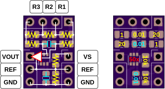
Three current sense resistors are placed in series so it can provide 3 different current ranges depending on which pins are used.
The middle resistor should be used for the highest current setting (smallest sense resistor) since this position is routed for the best kelvin connection.
The board includes an optional resistor divider to provide the reference voltage. This reference voltage should be connected to the negative input of a differential ADC. An additional reference pin is available if you want to provide the voltage externally.
The three sense resistors are connected between the pins of a 4 pin header. Run the current being measured between two adjacent pins. The current scale depends on the sense resistors installed between those pins.
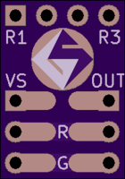
A three pin header is provided for power and reference input, and another three pin header provides amplifier and reference output.
The 16 bit differential ADC in NXP Kinetis MCUs are ideal for measuring the output. If you use the integrated ~1V reference, you get a +/- 1V range. Divide this by the gain of the amplifier (I suggest 50x version) and you get a 20mV full scale burden voltage. This 20mV divided by the value of the current sense resistor determines the full scale range. For example:
- 0.01 Ohm: +/-2A
- 1 Ohm: +/-20mA
- 20 Ohm: +/-1mA


