Set of information and tools whilst working with my M3i Zero (GMP-Z003) and
it's firmware. Use this information however you want.
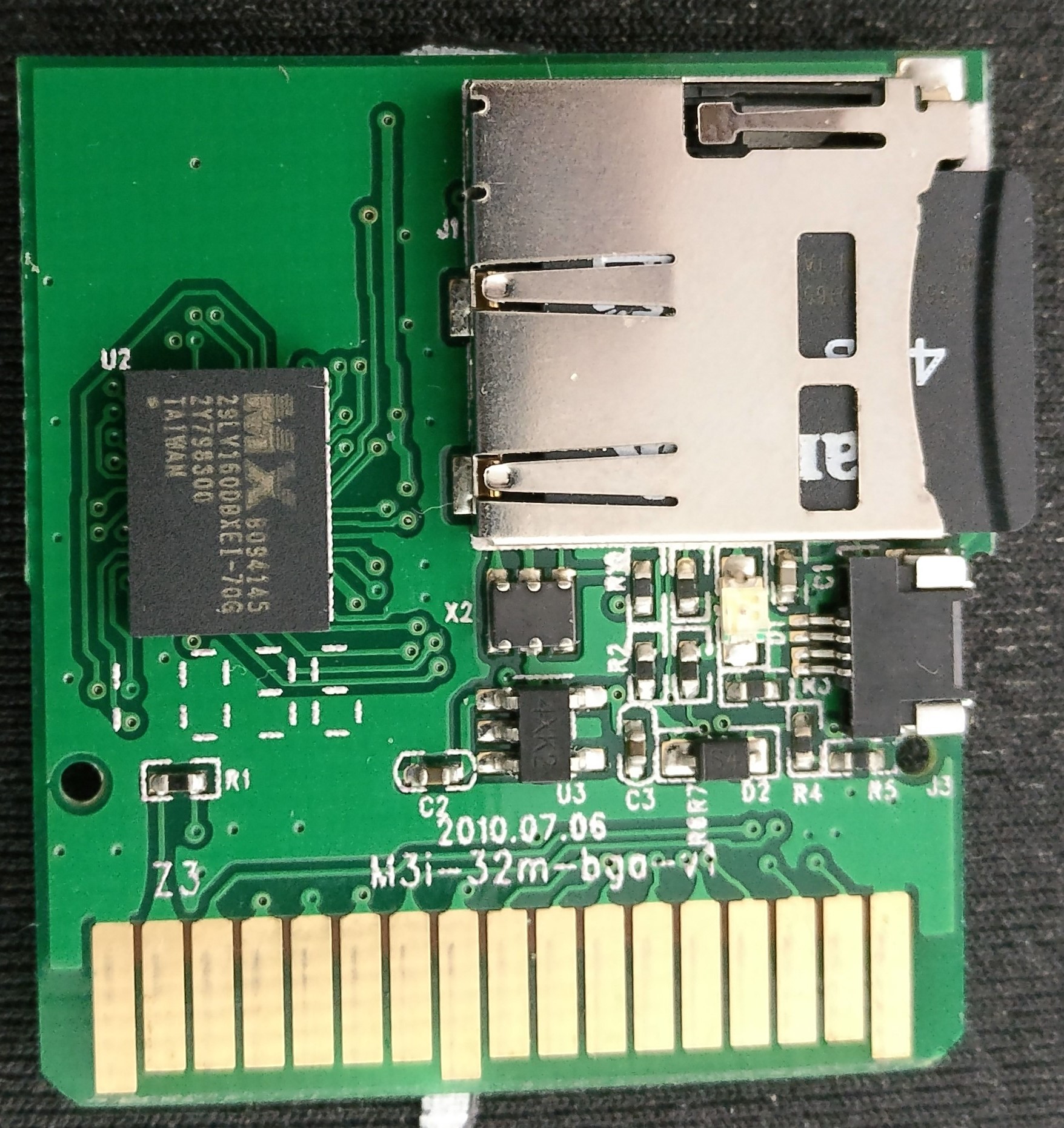
The GMP-Z003 uses a MX29LV160DBXEI-70G for flash memory, it is a 2MB chip.
This device operates over a voltage range of 2.7V to 3.6V typically using a 3V
power supply input. The flash memory is read directly to the NDS as a cartridge,
the format of which can be found here.
It is writeable through the flashing process.
The device can be flashed by providing DC power to the J3 port. I just stripped
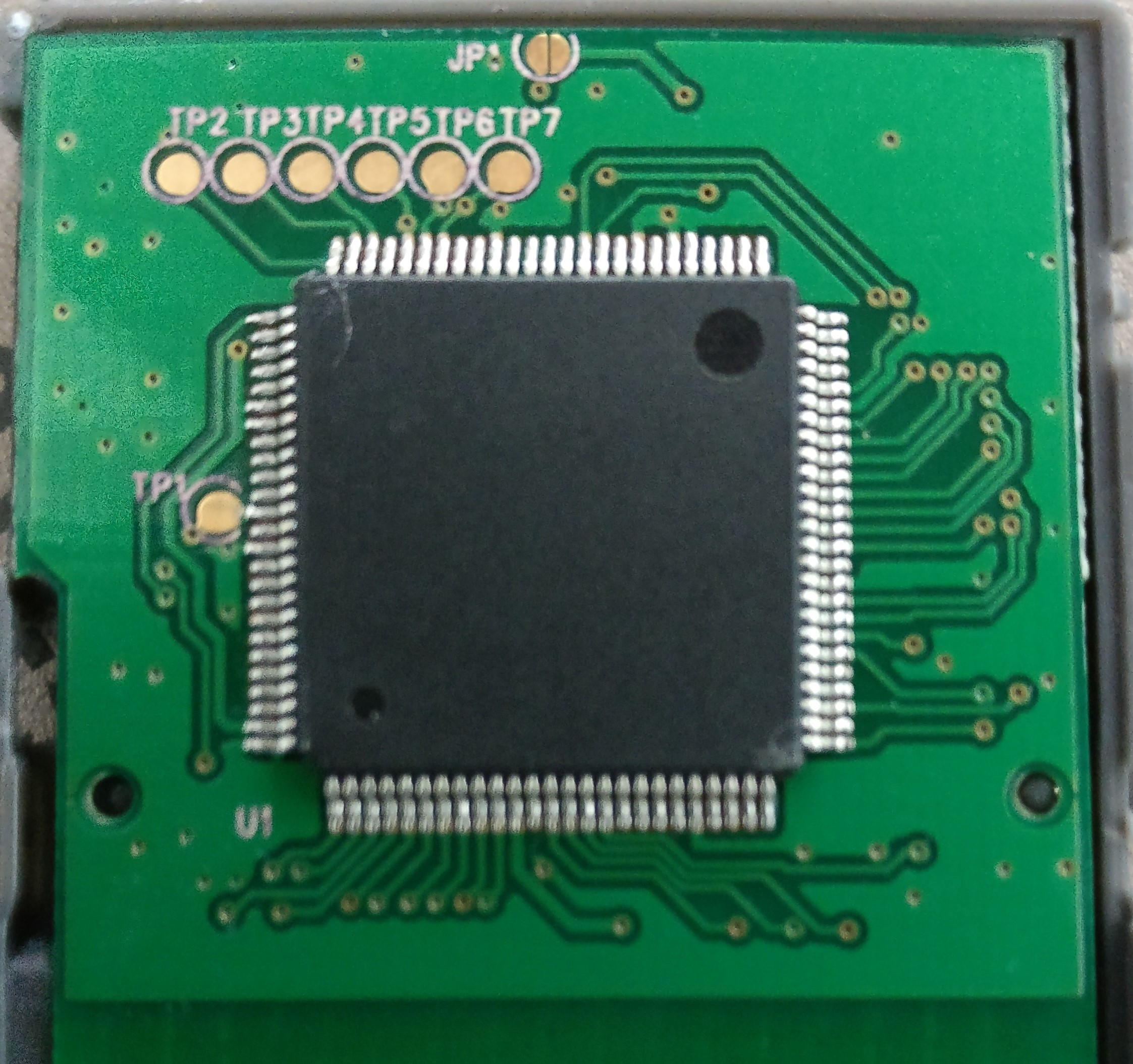
a USB cable and put the positive and ground in. The FPGA searches
the SD card for /F_CORE.DAT and copies 0x200000 -> 0x400000 to the flash
memory chip. I believe the F_CORE.DAT needs to be signed in order for the
FPGA to copy it first however.
The LED light D1 will change depending on the status of the flash:
- Nothing: No power or completed
- Static: Error reading
F_CORE.DAT(SD card might not be inserted, etc..) - Flashing: Copying
F_CORE.DATto the flash memory.
Alternatively the device can be flashed whilst inserted via the DS itself using card commands.
The common DLDI interface for the flash cart can be found here: G003.dldi And the reconstructed C source of that DLDI interface can be found here: iointerface.c
B0 00 00 00 00 00 00 00= Card Info (should be 0x5AA5)C9 oo oo oo oo xx 00 00= Read (FIFO read 0x200 words)C5 oo oo oo oo xx 00 00= Write (write 0x200 words)C6 00 00 00 00 00 00 00= get write status, read 1 word (= 0 when finished)CA 00 00 00 00 00 00 00= get read status, read 1 word (= 0 when finished)
Where oooooo is the offset in number of words(?), MSB first
Where xx represents the type in the DLDI interface this is set to 0x00 for SD card access.
0x00: SD card access afaik.0xE0: "SW" header, used with offset = 0, after that offset += 0x10000 (in number of words)0xF0: "SW" regular sector (0x200 bytes)0xA0: "HW" sector. One sector (header ?) is at 0x80000000 then the others start at offset 0.
- TuxSH for everything on card commands.

