Memory Design Workshop 2021
This repository reflects the work done in the lab sessions the Memory Design Workshop 2021 (MDW), offered by IEEE Banglore Section and IEEE CAS Banglore Chapter. The event was comprised of 5 days of lectures,2 in a day from Industry maestros and esteemed academicians, followed by self-paced hands-on lab session spanning over 2 weeks, aiming to familiarise ourselves with freeware tools, PDKs, Analog Design focusing on Memory Designs and Concepts.Table of Contents
About
This workshop presents a basic overview of different SRAM Cell Designs using LTSpice and ASU's Arizona State Predictive PDK (ASAP) 14nm FinFET node, using an intuitive approach to designing a simple SRAM Cells. This workshop also provides deep insights into recent advancements and current research trends in Memory Cell Designs. Here I have uploaded all the works done by me in 4 lab sessions organized by this workshop.
Lab 1
- Understand basic analysis types in LTSpice.
- Run an inverter transient and DC analysis.
- Assignment :
- Calculate the power of a nominally sized inverter driving a load of 1fF/5fF.
- Calculate Fan out of 1 (FO1) and Fan out of 4 (F04) delay of the nominally sized inverter at nominal and +/-10% supply.
- Calculate the leakage power of a 50fin inverter and compare it with a 22nm planar FET inverter of the same width.
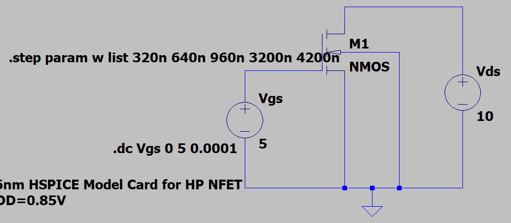
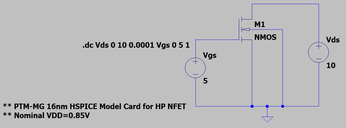
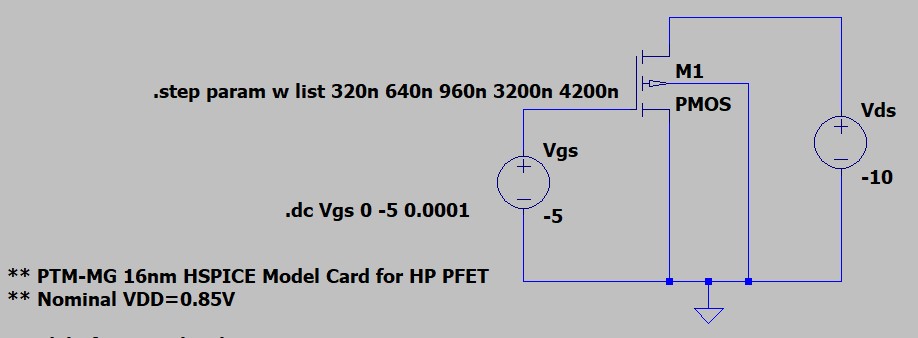
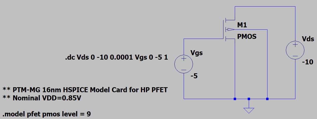
Schematic Diagram :
- NMOS: Id vs Vgs Schematic Diagram
- NMOS: Id vs Vds Schematic Diagram
- PMOS: Id vs Vgs Schematic Diagram
- PMOS: Id vs Vds Schematic Diagram
Resultant Waveform :
- NMOS: Id vs Vgs plots
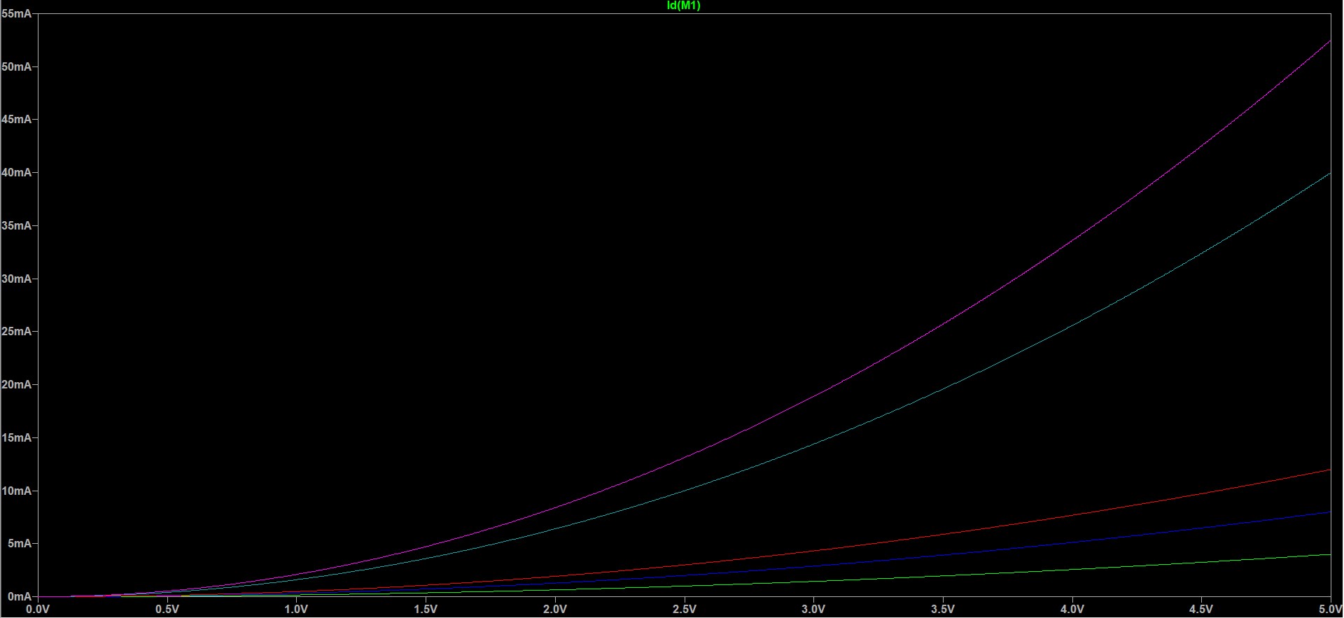
Different colors showing different values of Id when w = 320, 640, 960, 3200, 4200n - NMOS: Id vs Vds plots
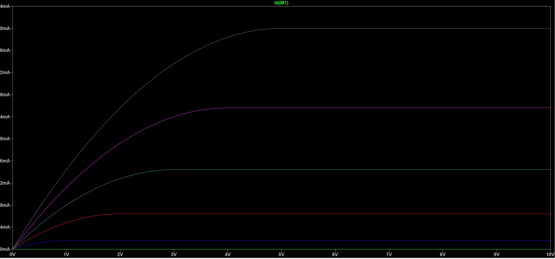
Different colors showing different values of Id when Vgs = 0, 1, 2, 3, 4, 5 V - PMOS: Id vs Vgs plots

Different colors showing different values of Id when w = 320, 640, 960, 3200, 4200n - PMOS: Id vs Vds plots
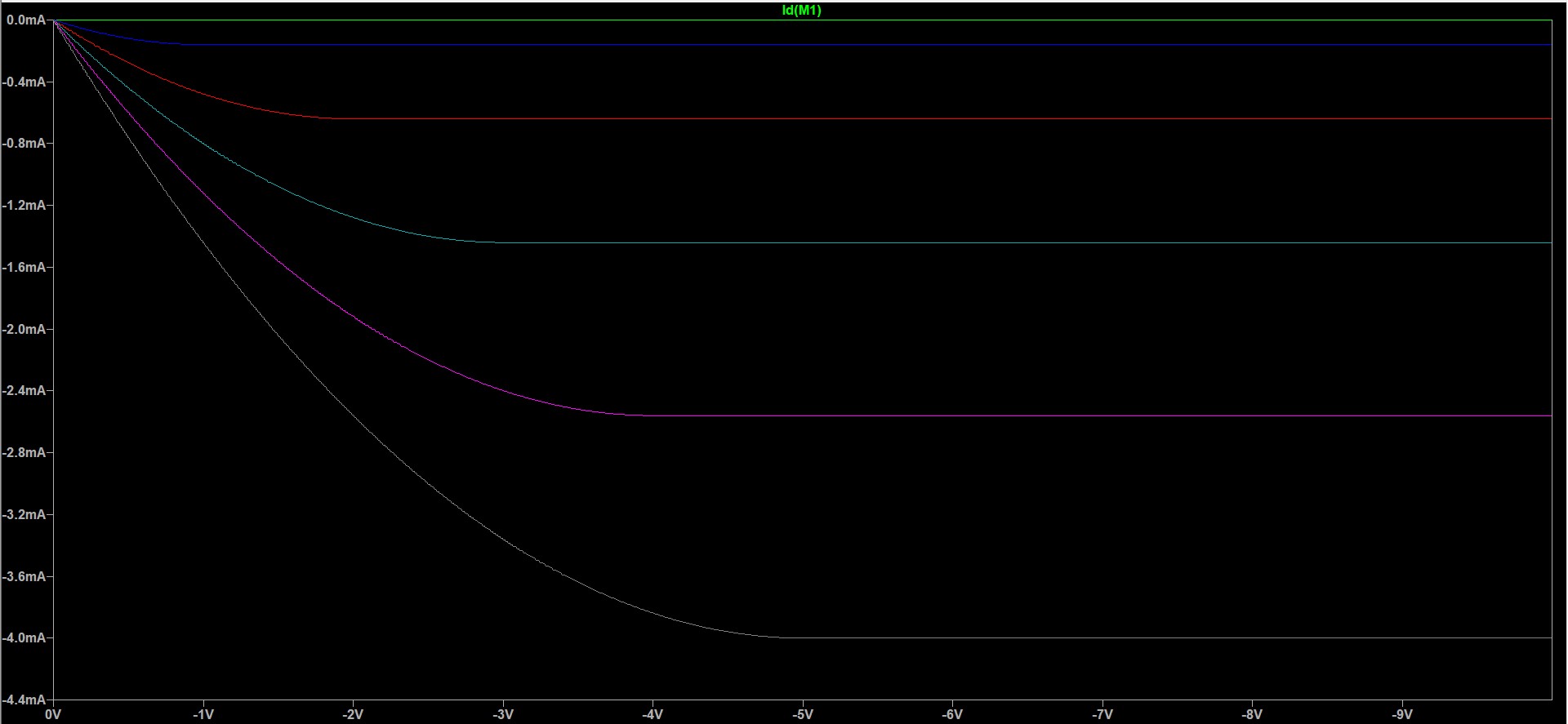
Different colors showing different values of Id when Vgs = 0, 1, 2, 3, 4, 5 V
Lab 2
- Run an inverter transient and DC analysis.
- Assignment :
- Calculate the power of a nominally sized inverter driving a load of 1fF/5fF.
- Calculate Fan out of 1 (FO1) and Fan out of 4 (F04) delay of the nominally sized inverter at nominal and +/-10% supply.
- Calculate the leakage power of a 50fin inverter and compare it with a 22nm planar FET inverter of the same width.
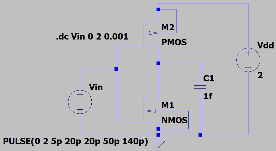
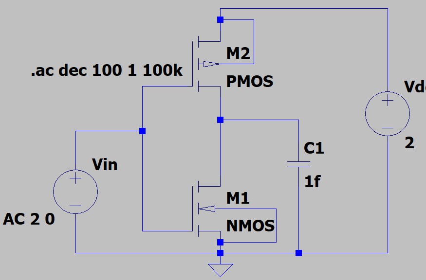
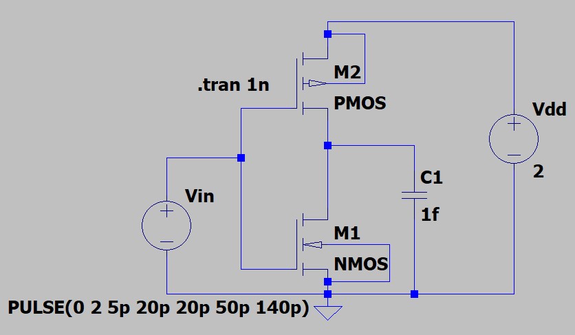
Schematic Diagram :
Resultant Waveform :
- CMOS Inverter Waveform
DC Analysis
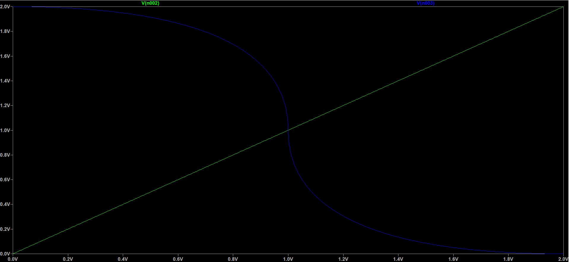
AC Analysis
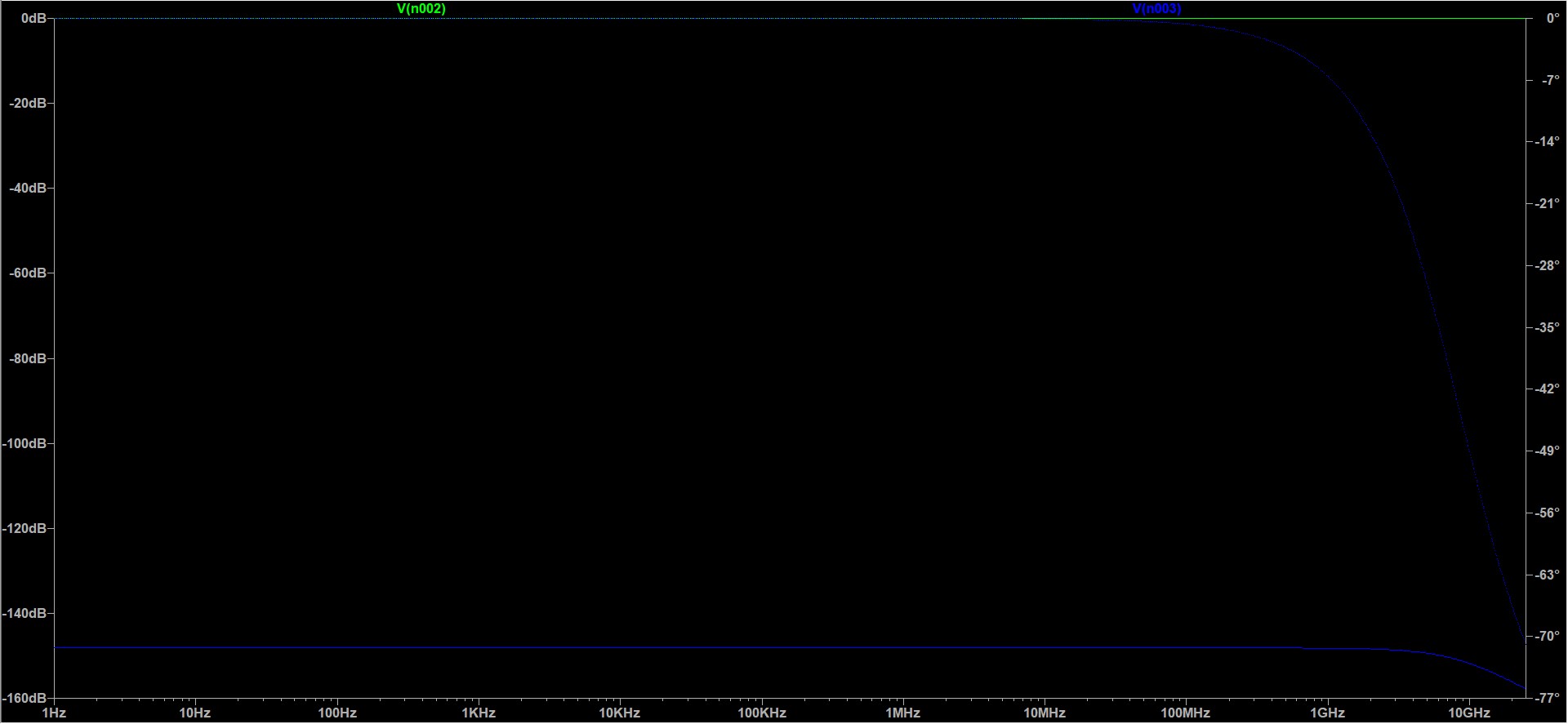
Transient Analysis
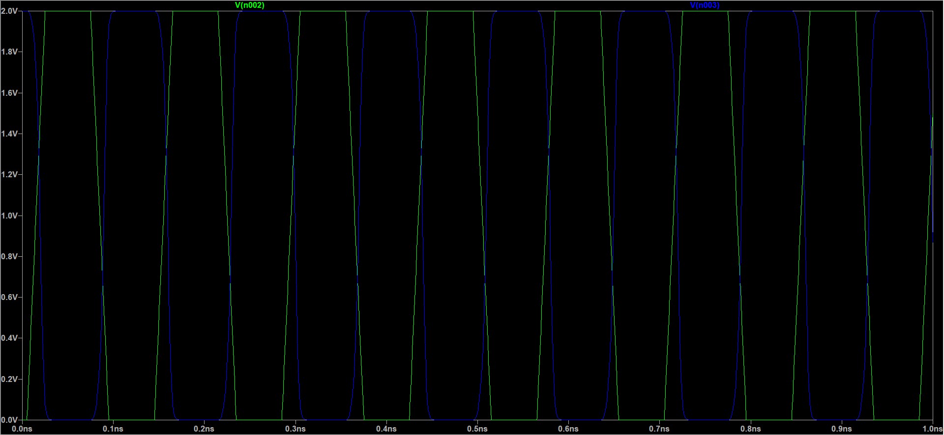
- Power Analysis
Load = 1fF
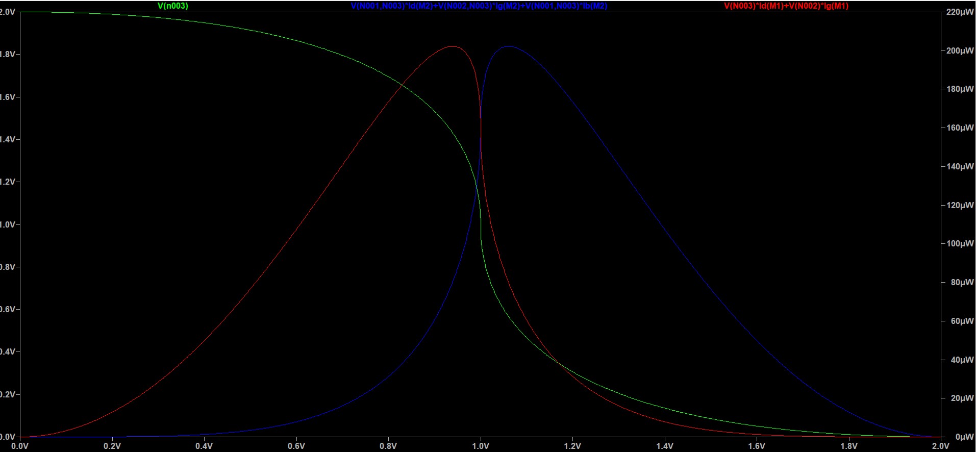
Total Power consumed by CMOS Inverter = 201.78 μW (PMOS) + 202.57 μW (NMOS)
Load = 5fF
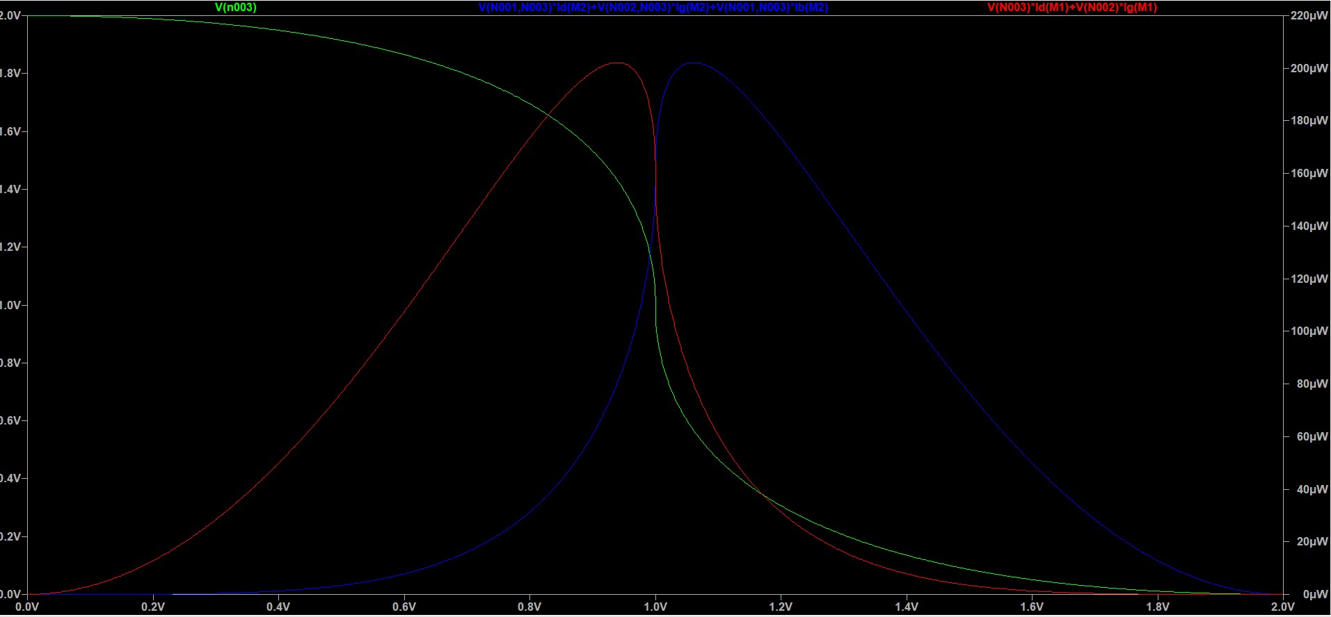
Total Power consumed by CMOS Inverter = 202.57 μW (PMOS) + 202.83 μW (NMOS)
Lab 3
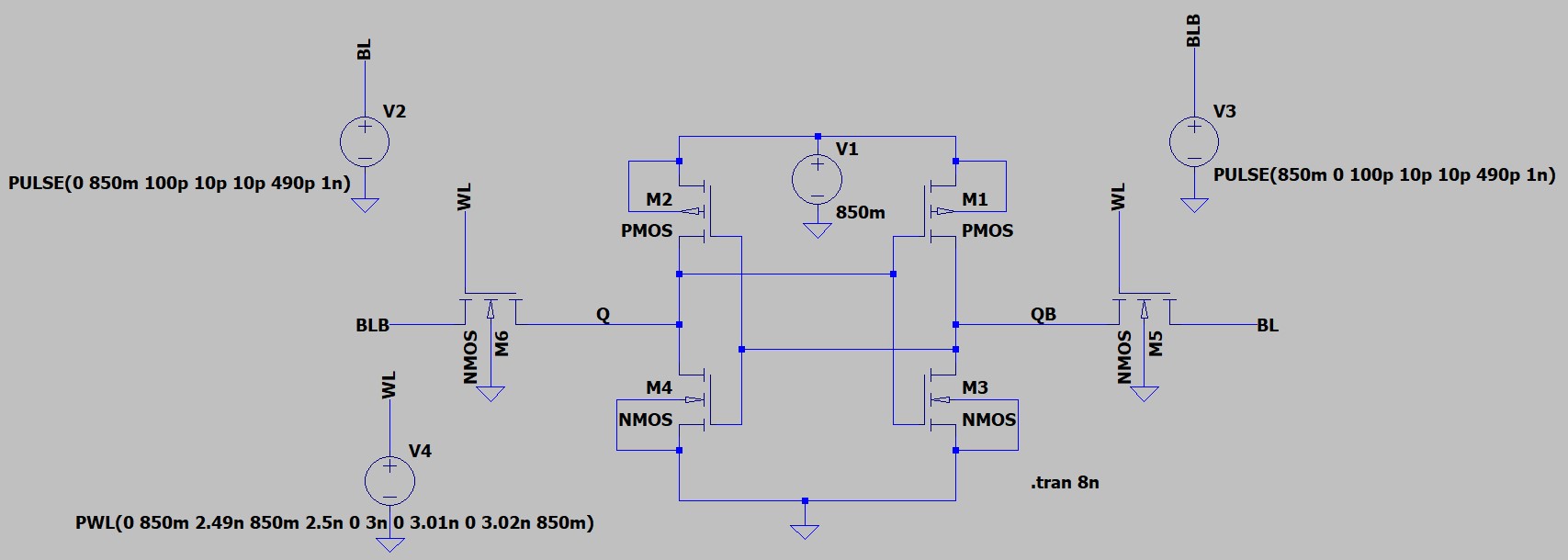
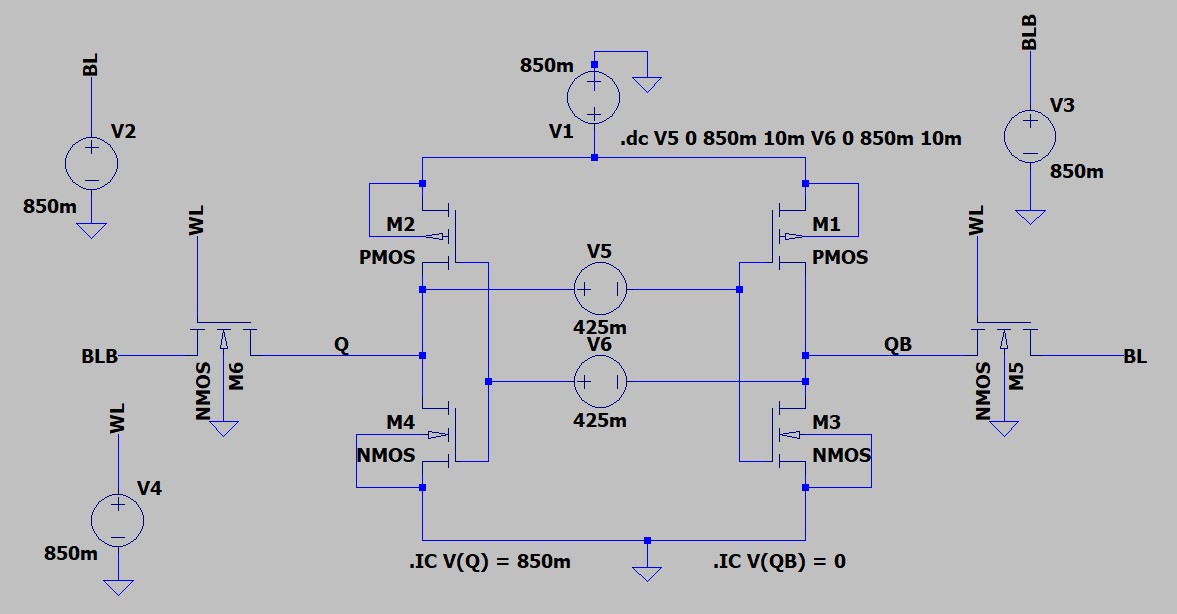
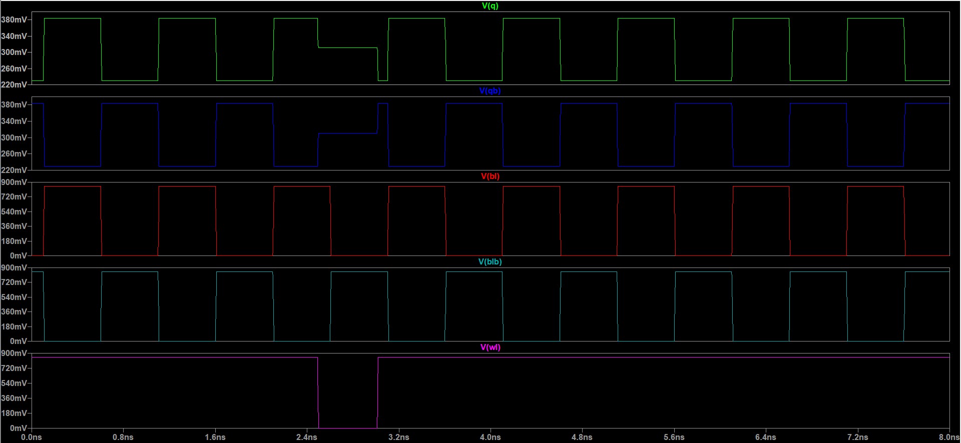
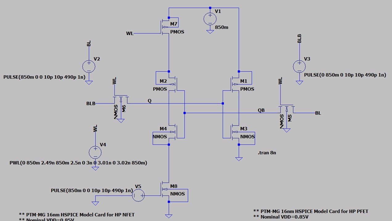
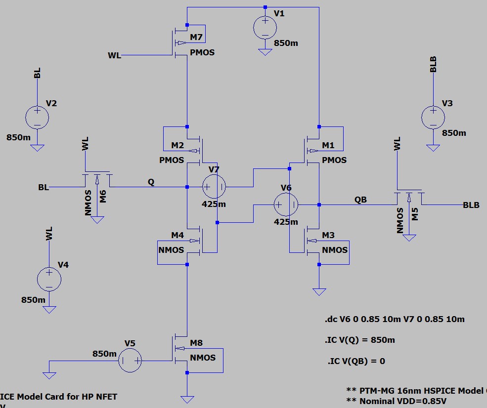
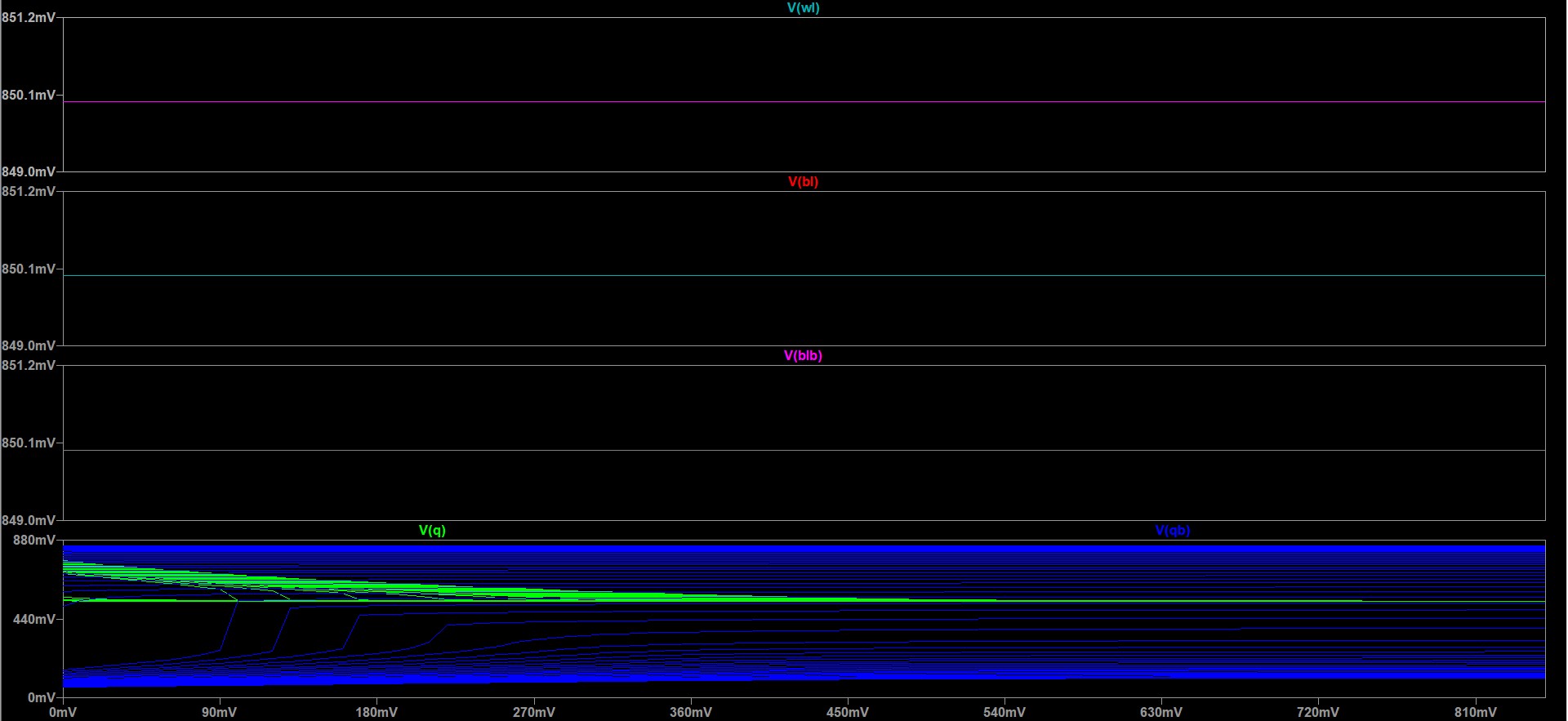
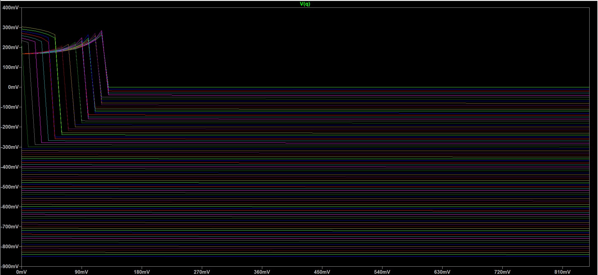
- Desing and Analysis of 6T SRAM Cell.
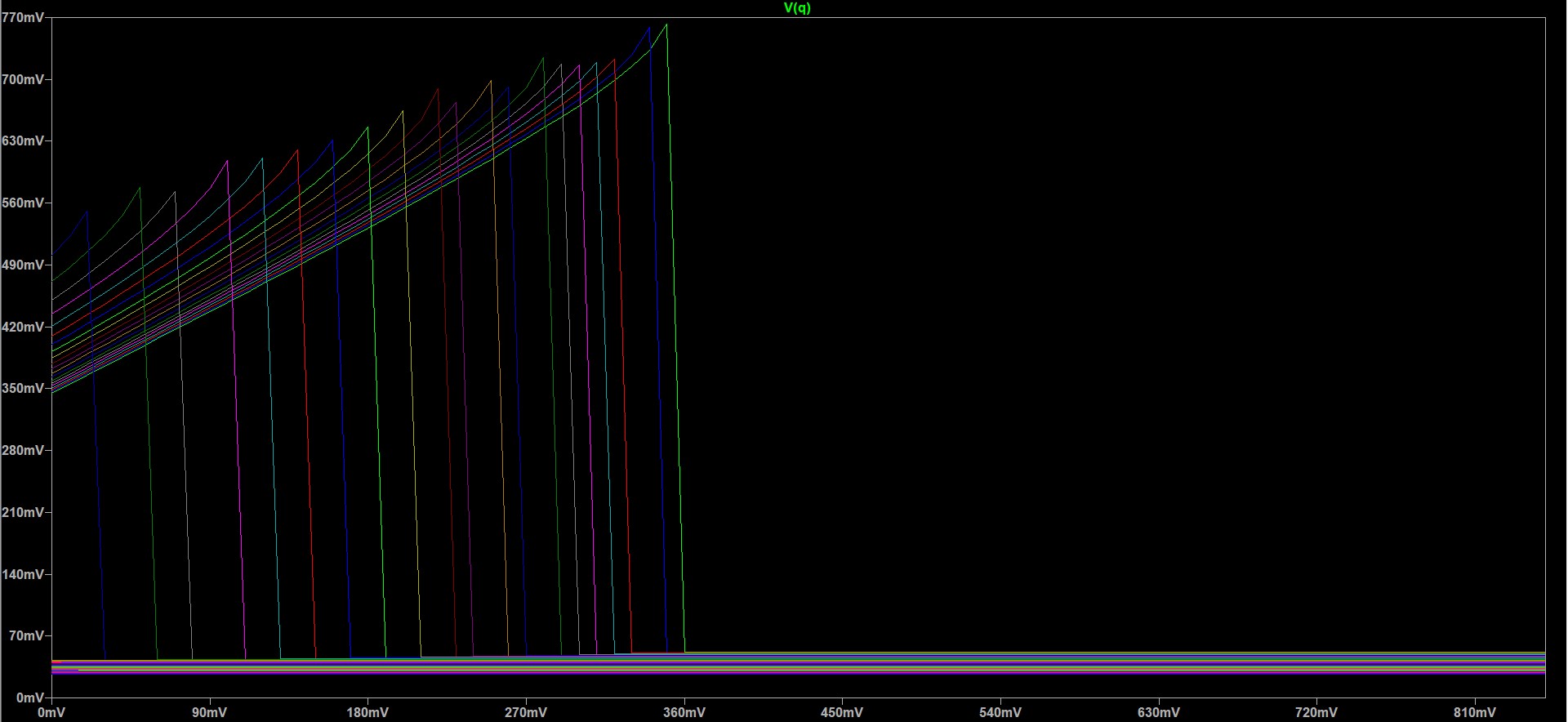
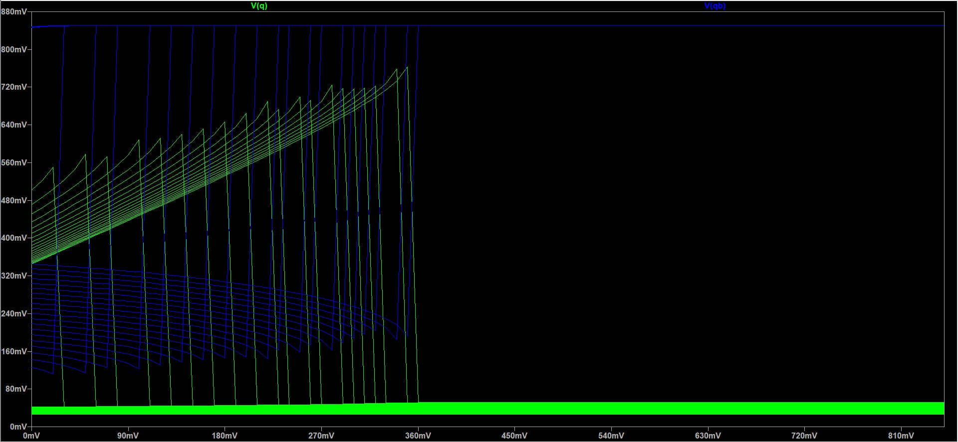
- Perform Static-noise margin analysis of the same refer to this "Static-noise margin analysis of MOS SRAM cells" and Link
Schematic Diagram :
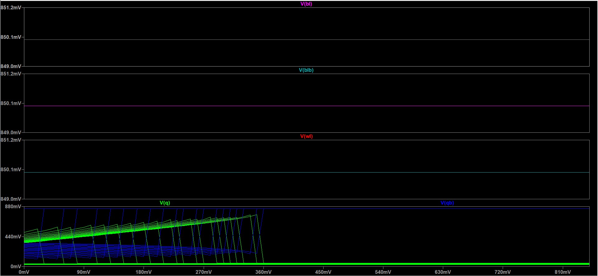
Resultant Waveform :
Lab 4
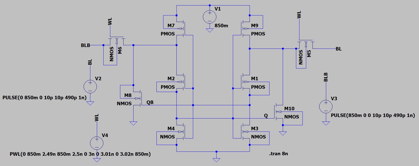
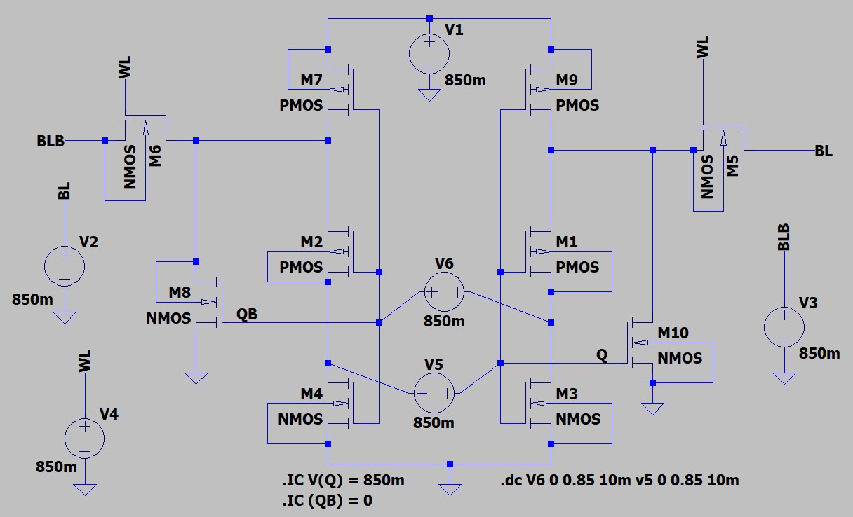
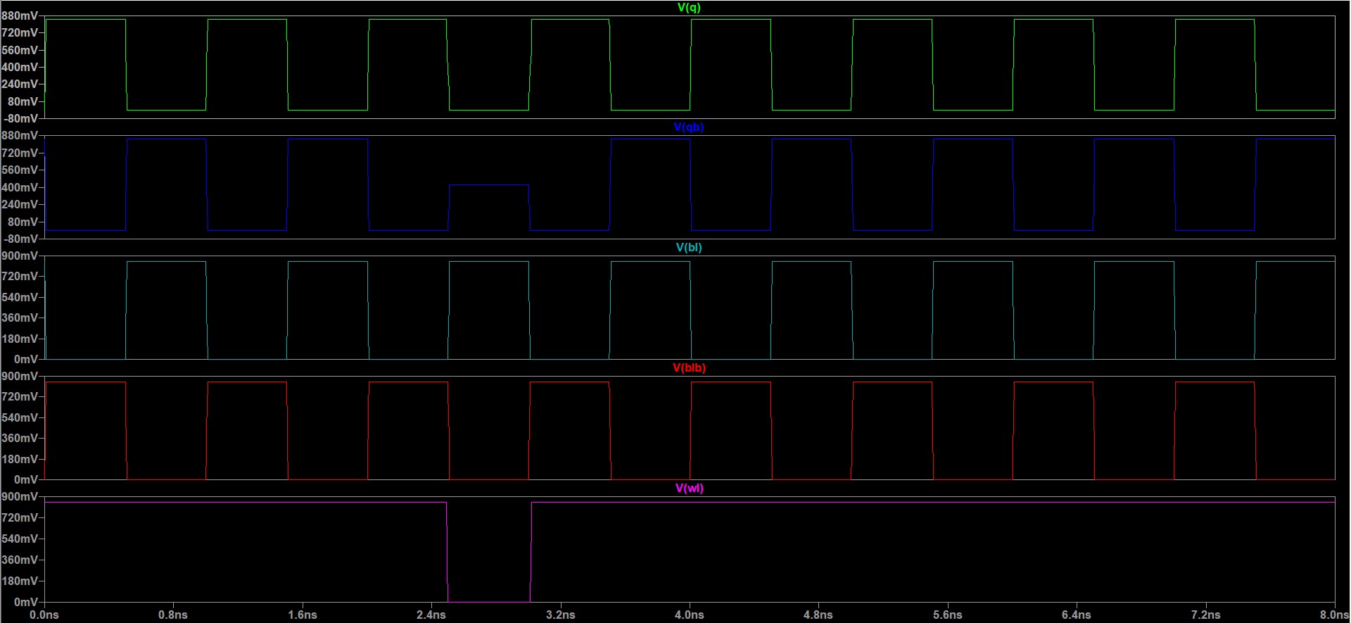
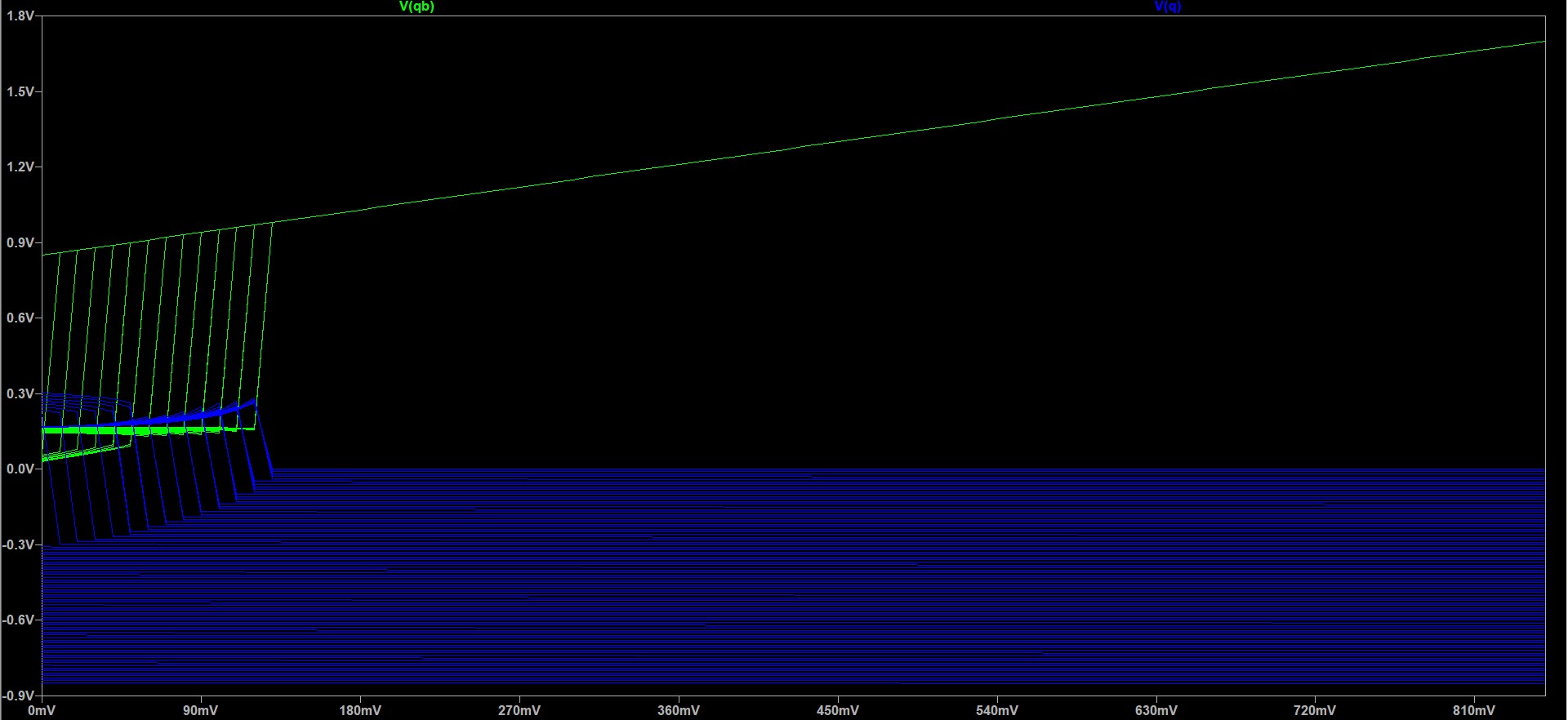
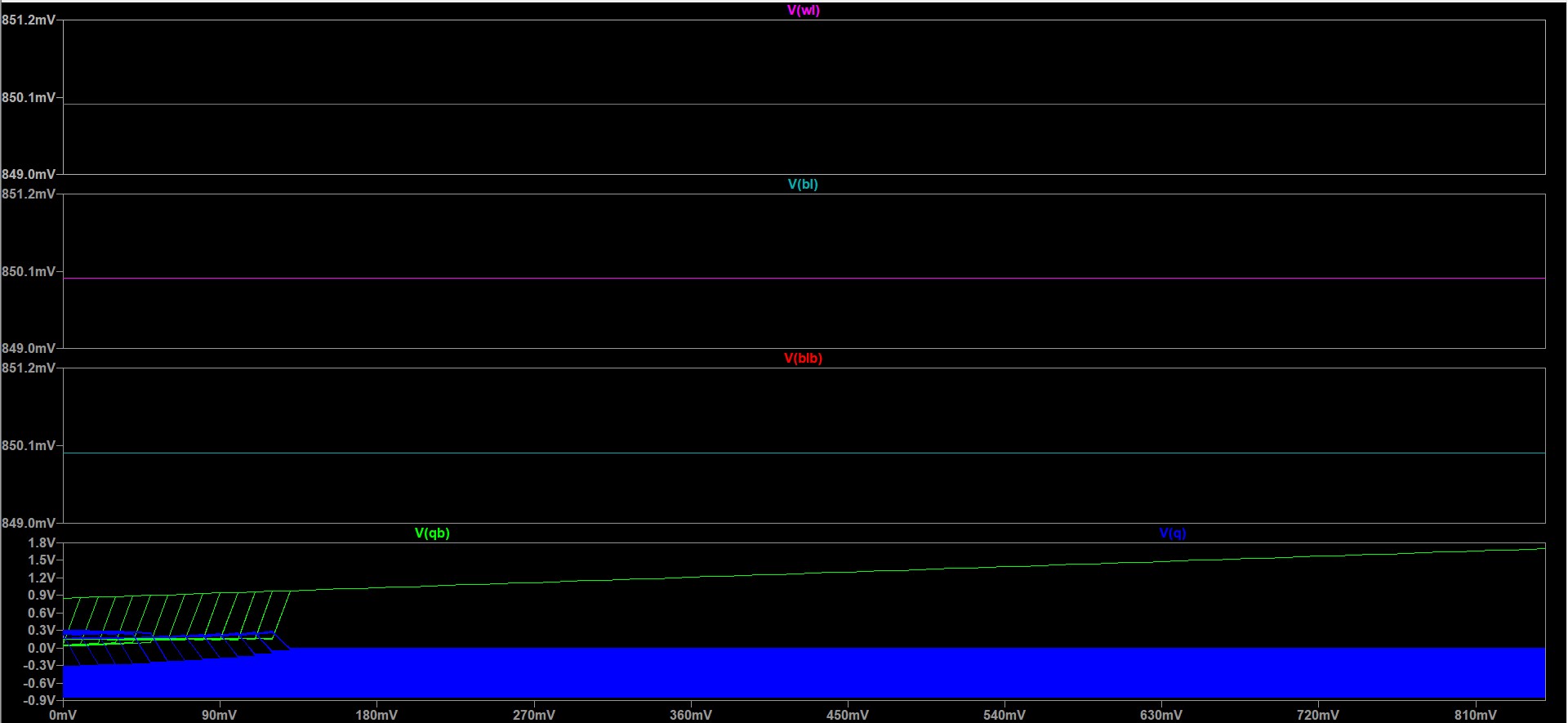
- Desing and Analysis of 8T and 10T SRAM Cell.
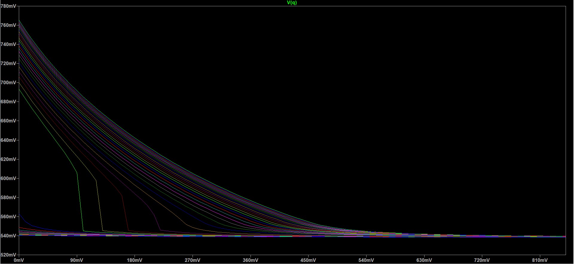
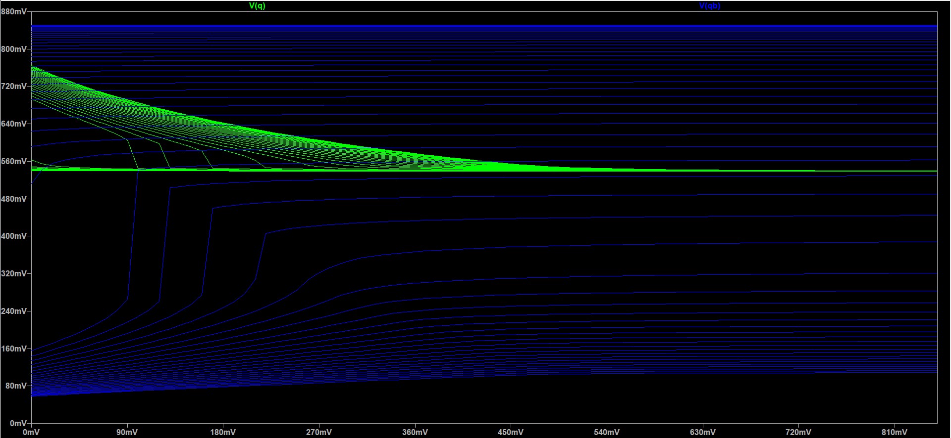
- Perform Static-noise margin analysis of the same refer to this "Static-noise margin analysis of MOS SRAM cells" and Link
Schematic Diagram :
Resultant Waveform :
Future Scope
- Work on getting specifications and change your designs according to them.
- After changing in your design, make this design as your own IP.
- Design Layouts and Verify them with LVS and DRC Checks.

