This workshop presents a basic overview of different SRAM Cell Designs using LTSpice and ASU's Arizona State Predictive PDK (ASAP) 14nm FinFET node, using an intuitive approach to designing a simple SRAM Cells. This workshop also provides deep insights into recent advancements and current research trends in Memory Cell Designs. Here I have uploaded all the works done by me in 4 lab sessions organized by this workshop.
- Understand basic analysis types in LTSpice.
- Run an inverter transient and DC analysis.
- Assignment :
- Calculate the power of a nominally sized inverter driving a load of 1fF/5fF.
- Calculate Fan out of 1 (FO1) and Fan out of 4 (F04) delay of the nominally sized inverter at nominal and +/-10% supply.
- Calculate the leakage power of a 50fin inverter and compare it with a 22nm planar FET inverter of the same width.
Schematic Diagram :
- NMOS: Id vs Vgs Schematic Diagram
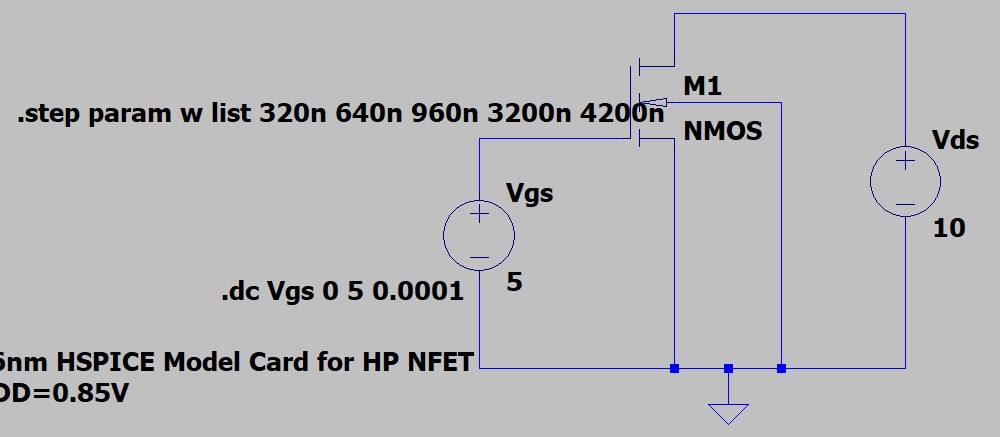
- NMOS: Id vs Vds Schematic Diagram

- PMOS: Id vs Vgs Schematic Diagram
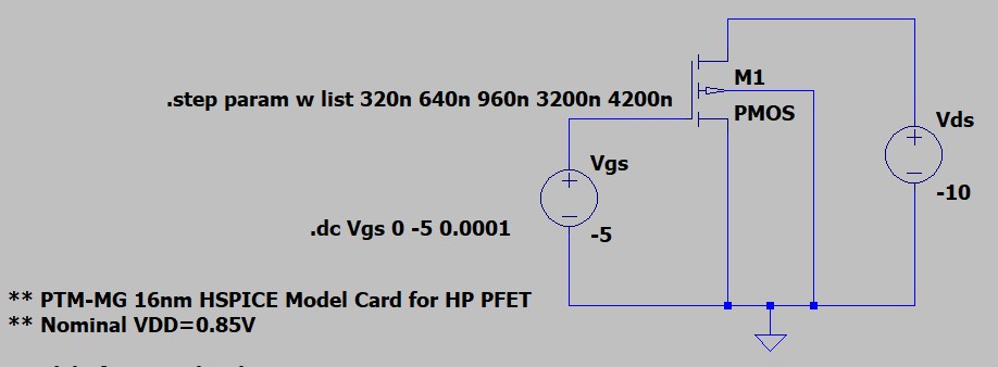
- PMOS: Id vs Vds Schematic Diagram
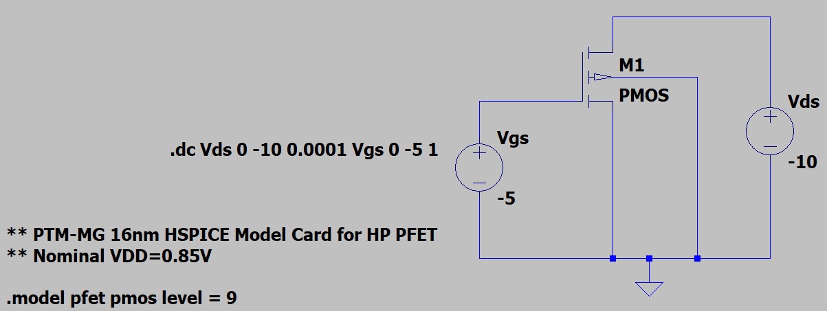
Resultant Waveform :
- NMOS: Id vs Vgs plots
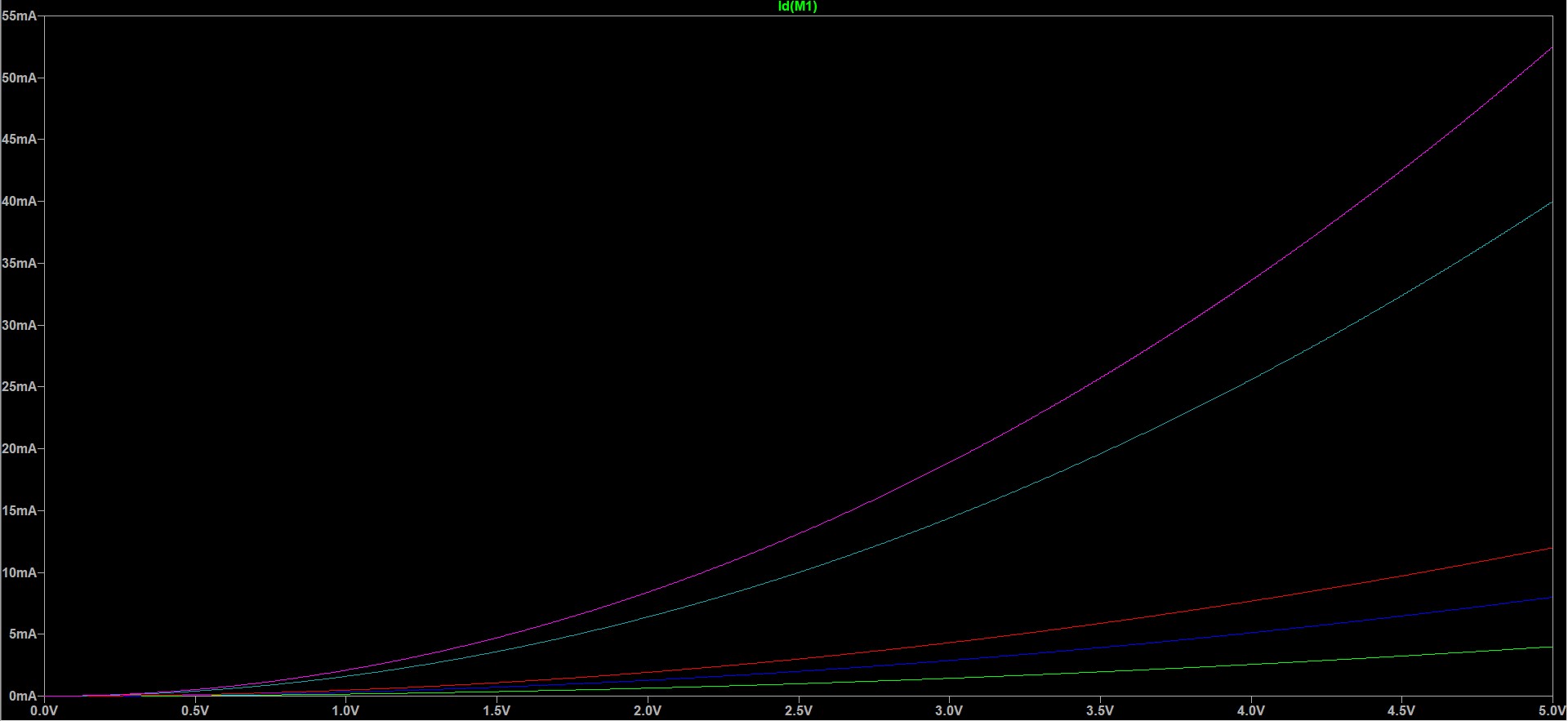
Different colors showing different values of Id when w = 320, 640, 960, 3200, 4200n - NMOS: Id vs Vds plots

Different colors showing different values of Id when Vgs = 0, 1, 2, 3, 4, 5 V - PMOS: Id vs Vgs plots

Different colors showing different values of Id when w = 320, 640, 960, 3200, 4200n - PMOS: Id vs Vds plots

Different colors showing different values of Id when Vgs = 0, 1, 2, 3, 4, 5 V
- Run an inverter transient and DC analysis.
- Assignment :
- Calculate the power of a nominally sized inverter driving a load of 1fF/5fF.
- Calculate Fan out of 1 (FO1) and Fan out of 4 (F04) delay of the nominally sized inverter at nominal and +/-10% supply.
- Calculate the leakage power of a 50fin inverter and compare it with a 22nm planar FET inverter of the same width.
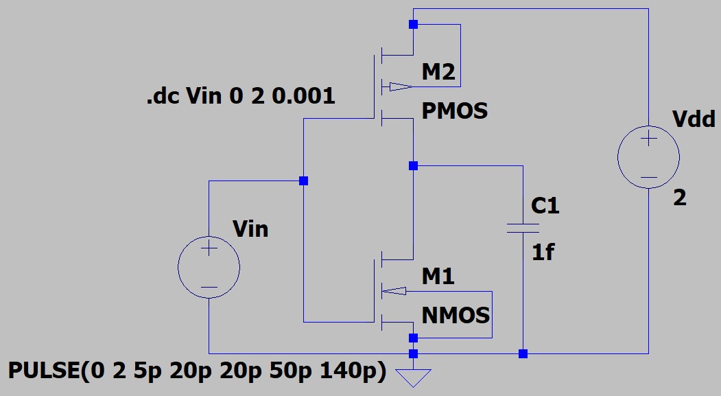
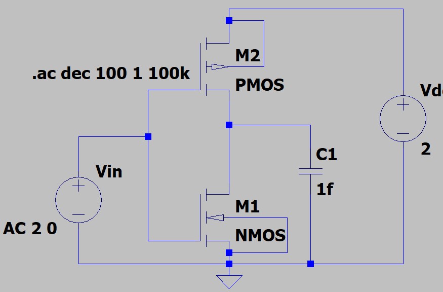
Schematic Diagram :
Resultant Waveform :
- CMOS Inverter Waveform
DC Analysis

AC Analysis

Transient Analysis
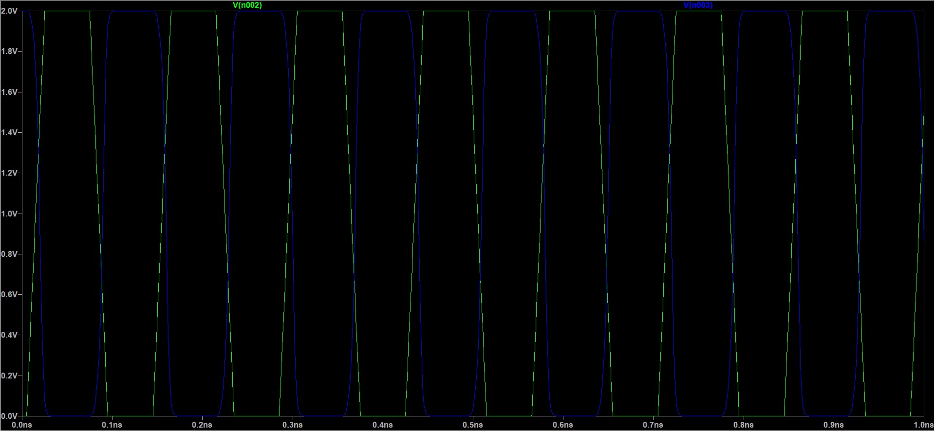
- Power Analysis
Load = 1fF
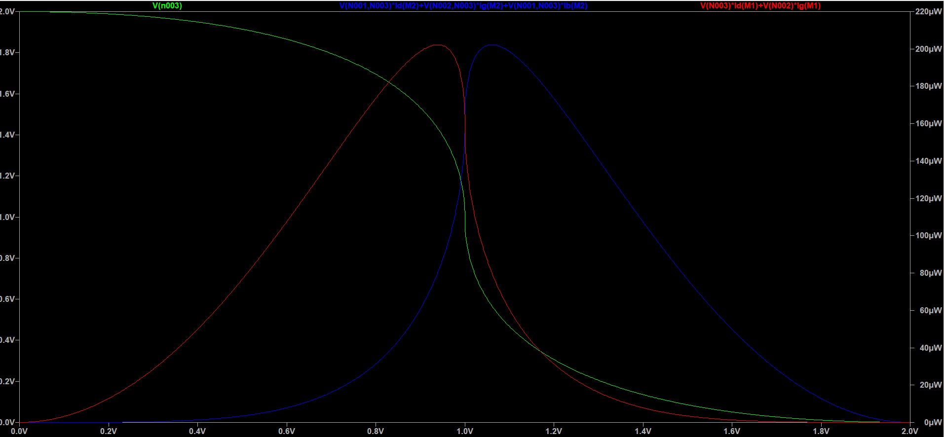
Total Power consumed by CMOS Inverter = 201.78 μW (PMOS) + 202.57 μW (NMOS)
Load = 5fF

Total Power consumed by CMOS Inverter = 202.57 μW (PMOS) + 202.83 μW (NMOS)
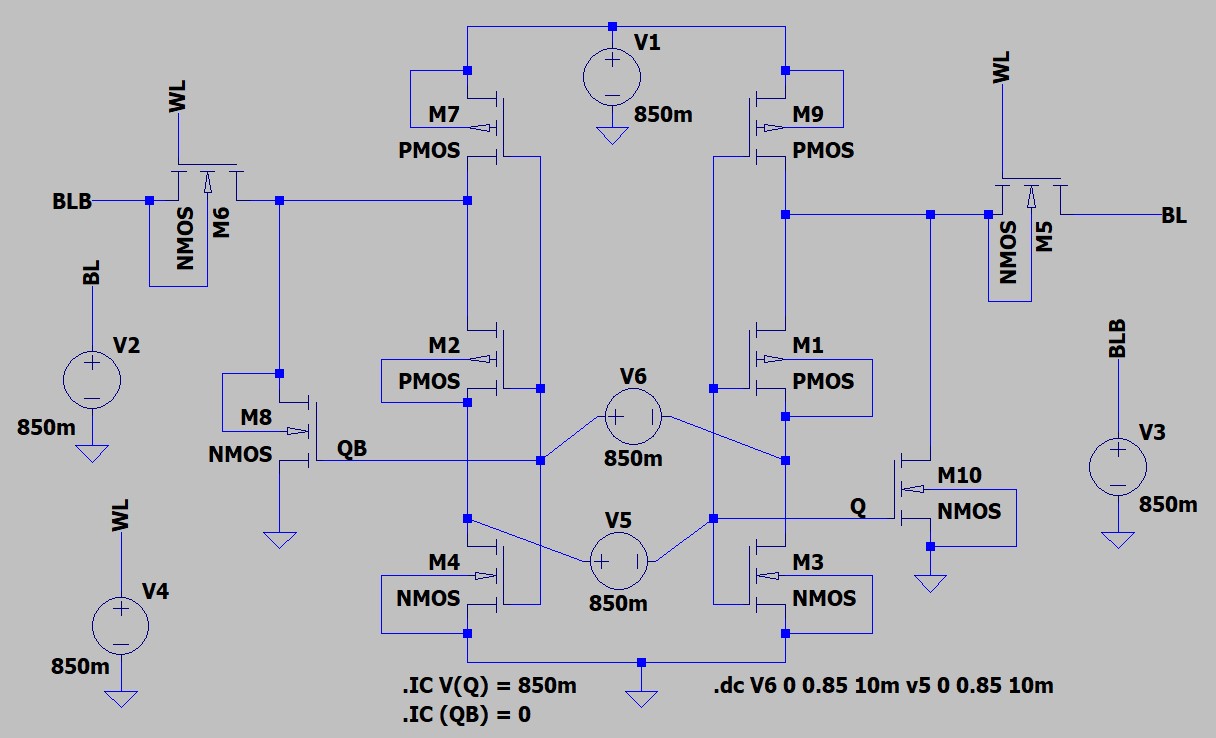
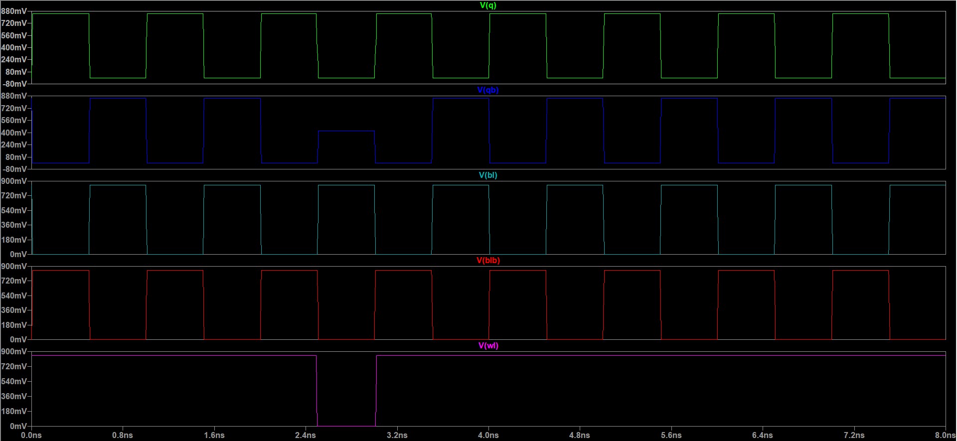
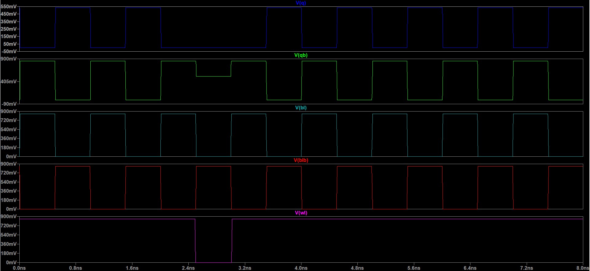
- Desing and Analysis of 6T SRAM Cell.
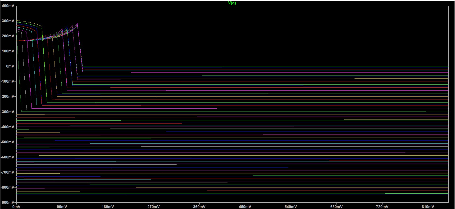
- Perform Static-noise margin analysis of the same refer to this "Static-noise margin analysis of MOS SRAM cells" and Link
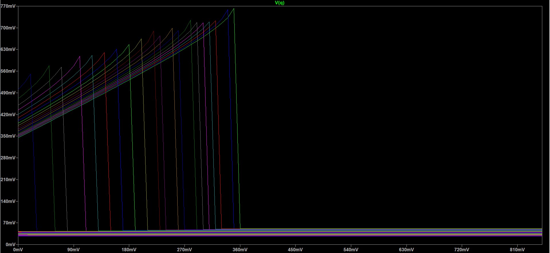
Schematic Diagram :
Resultant Waveform :
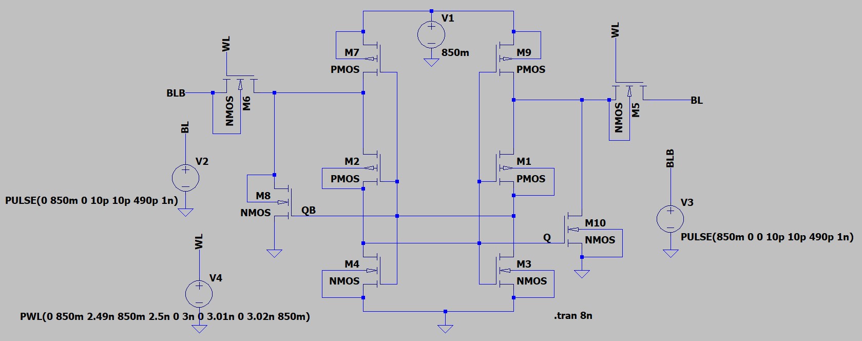
- Desing and Analysis of 8T and 10T SRAM Cell.
- Perform Static-noise margin analysis of the same refer to this "Static-noise margin analysis of MOS SRAM cells" and Link
Schematic Diagram :
Resultant Waveform :
- Work on getting specifications and change your designs according to them.
- After changing in your design, make this design as your own IP.
- Design Layouts and Verify them with LVS and DRC Checks.

