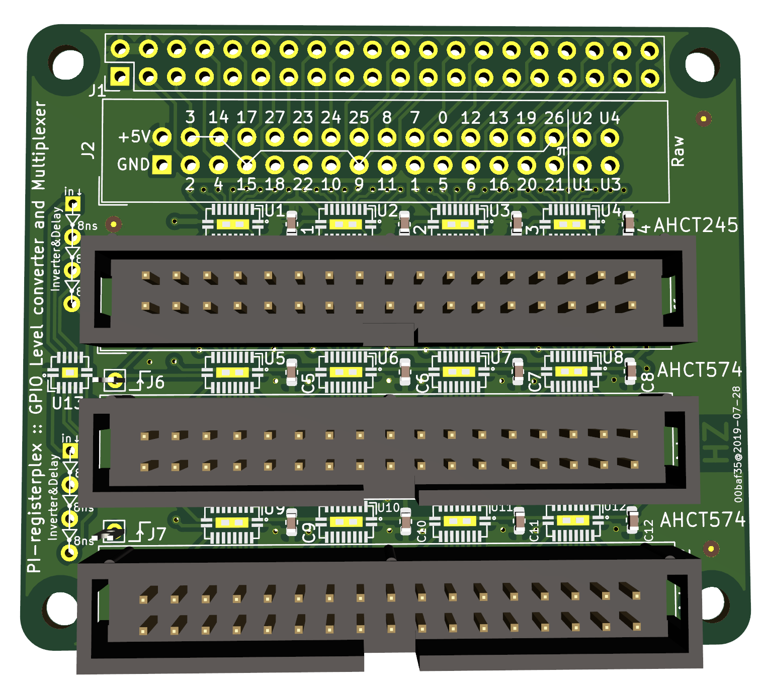
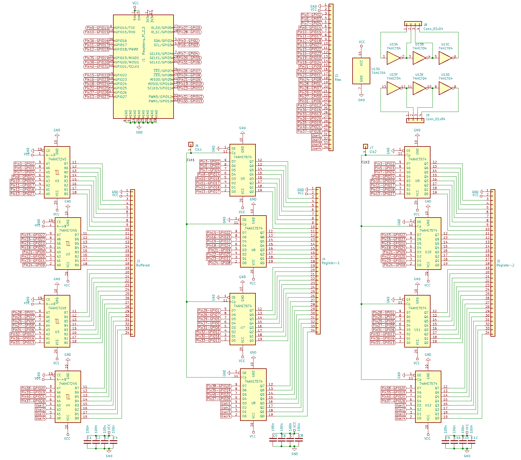
- 1x32 'raw' output of GPIO pins, or inputs if not used with a Pi
- 1x32 bit buffer (AHCT245) to buffer all 28 GPIO bits plus 4 user bits
- 2x32 bit registers (AHCT574) with user-choice of clock.
- 6 NOT gates that can be used to use as clock inverter and play with gate delays.
This board directly plugs into the Rasbperry Pi and can be used as a GPIO multiplexer with that, but the raw inputs are also available directly, so this can be used in any project. The 34 pin connectors have the same pinout throughout: +5V and GND followed by 32 bits of data.
Using the AHCT gates allows to voltage convert 3.3V logic levels to 5V.
The chip packages are DHVQFN20, which allows for compact design and is still somewhat easy to solder if you use a stencil.
| Chip | Package | Vendor type example |
|---|---|---|
| 74AHCT245 | DHVQFN20 (SOT764-1) | NXP 74AHCT245BQ,115 |
| 74AHCT574 | DHVQFN20 (SOT764-1) | NXP 74AHCT574BQ,115 |
| 74AHCT04 | DHVQFN14 (SOT762-1) | NXP 74AHCT04BQ,115 |
The clocks (J6 and J7) of the registers are not connected by default, so
it allows you to choose any GPIO output or other signal to clock in the
registers.
The buffer and registers are for 32 bits, but we only have 28 GPIO outputs.
The remaining bits are passed through as user bits (U1 ... U4) from inputs
on the J2 'Raw' header.
PCB is shared on OshPark.
Pick two GPIO lines as a clock to connect to J6 and J7 allows to write
to the registers. Straight forward:
- write Datum1, transition clock2
¯╲_ - transition clock1
_╱¯(clocks in Datum1) - Write Datum2, transition clock1
¯╲_ - transition clock2
_╱¯(clocks in Datum2)
In this case, the inverter gates are not needed.
Chose one GPIO as clock and wire it up to an inverter. Wire up one of the 574's directly to the pin, and the other through the inverter.
- Write Datum1
- transition clock
_╱¯(clocks in Datum1) - Write Datum2
- transition clock
¯╲_(the inverted signal clocks in Datum2)
Same as above, but only one clock line needed.
Wire up the Clock line to at least one inverters, maybe more in one chain to
create some delay. Let's call this Clock'. Take the output of that through
another inverter, let's call this Clock''. Connect these to J6 and J7.
- Clock in Datum1 and with it transition
Clock_╱¯. The delayed clock prime that transitions to positive a few nanoseconds later will clock in the data. - Clock in Datum2 and with it transition
Clock¯╲_. The inverted clock from (1) now transitions to positive a few nanoseconds later will clock in the data.
Each write write will store one datum. Using the gates as delay line and inverter, no separate cycle is needed, each swing of the clock generates a store.
This is dangerous of course: it is not necessarily stable as we rely on the delay to be long enough for the D-FlipFlops set-up time, and this will highly depend on the chip manufacturer, temperature, age, ... Maybe use RC + AHCT14 or LV14 Schmitt-Trigger for a more defined delay ?

