The iCEBreaker FPGA board is a low cost, open-source educational FPGA development board.
The main motivating application of this board is for classes and workshops teaching the use of the open source FPGA design flow using Yosys, nextpnr, icestorm, iverilog, symbiflow and others. This means the board has to be low cost and have a nice set of features to allow for the design of interesting classes and workshop exercises. At the same time we want to allow the user to use the proprietary vendor tools if they choose to. Because of that we need to be compatible with their firmware upload tools.
-
iCE40UP5K in QFN48 (SG48) package
- iCE40 UltraPlus 5K
- 5280 Logic Cells (4-LUT + Carry + FF)
- 128 KBit Dual-Port Block RAM
- 1 MBit (128 KB) Single-Port RAM
- PLL, Two SPI and two I2C hard IPs
- Two internal oscillators (10 kHz and 48 MHz)
- 8 DSPs (16x16 multiply + 32 bit accumulate)
- 3x 24mA drive and 3x hard PWM IP
-
QSPI-DDR-capable flash 128 MBit (16 MB)
- We selected to use the Winbond W25Q128JVSIM
- We want to enable projects that access the flash and we want to provide the highest flash access speed possible.
-
FT2232H interface (microUSB plug)
- programming compatible with iCEstick and HX8K board
- works with Dimond Programmer and iceprog
- serial port compatible with iCEstick and HX8K breakout board
- 12 MHz XTAL oscillator (shared with FPGA)
- Solder jumpers to offer direct SRAM programming (like on HX8K breakout board)
- programming compatible with iCEstick and HX8K board
-
39 I/O capable pins:
- 4 pins for config (SDI, SDO, SCK, CSB)
- Either loading config from on board FLASH chip or provided through the FTDI chip with direct SRAM config.
- 2 extra GPIO pins for QSPI
- Together with the config pins, allows storage of additional data in the FLASH chip, and high speed QSPI DDR access. For example picosoc firmware.
- 3 PINs for RGB LED (pin header)
- 2 LEDs (one on output-only PLL pin)
- 1 Clock pin (on PLL GBIN)
- 1 UART Rx Pin via FTDI
- 1 UART Tx Pin via FTDI
- 1 Push Button
- 16 PINs on dual PMOD
- 8 PINs on single PMOD / snap-off section
- 4 pins for config (SDI, SDO, SCK, CSB)
-
Support for FTDI Async FIFO mode
- We want to support FTDI Async mode via some (unpopulated by default) zero ohm resistors
- This shares 8 GPIOs with the single PMOD / snap-off section
- This would also enable use of full list of RS232 signals
- BDATA[0] -- Tx on FTDI / Rx on FPGA (always connected, no zohm resistor required)
- BDATA[1] -- Rx on FTDI / Tx on FPGA (always connected, no zohm resistor required)
- BDATA[7:2] -- Shared with snap-off section (via zohm resistor footprint)
- RX Full -- Shared with snap-off section (via zohm resistor footprint)
- TX Empty -- Shared with snap-off section (via zohm resistor footprint)
- Read -- Shared with LED 1 (via zohm resistor footprint, LED used as RX indicator)
- Write -- Shared with LED 2 (via zohm resistor footprint, LED used as TX indicator)
- WakeUp -- Shared with Push Button (via zohm resistor footprint)
- This configuration uses the following pins when the jumpers ore reconfigured:
- The two on board red and green LED pins
- The on board user button pin
- snap off section single PMOD pins
-
Snap-off section (convertible to PMOD host / PMOD device)
- 5 LEDs in similar arrangement to iCEstick
- 3 Push Buttons
-
Other stuff
- Status LEDs for Power and CDONE (Configuration DONE)
- Header with supply rails: 5V, 3V3, 1V2, GND
- Debug header for all 6 QSPI pins
- Test points for UART Rx / Tx signals
- Jumpers or zohm resistors on all rails for measuring currents
- Four 3mm mounting holes on the main section and two more on the snap-off section
- The two LEDs on the main section should be wired "active low" so they work well as indicator LEDs for FIFO read/write.
- The five LEDs on the snap-off section should be wired "active high"
- A zohm resistor for Bank 2 supply so that the IO voltage can be changed. Use Bank 2 for one of the ports on the double PMOD.
- There should be auxilary 5V pin headers available for the PMODs. Some PMOD need either higher voltage or need to regulate their own voltage from 5V.
-
Unpopulated parts shipped with the board
- 3x Host PMOD (2x for dual PMOD port, 1x for snap-off section)
- 1x Device PMOD (for other side of snap-off section)
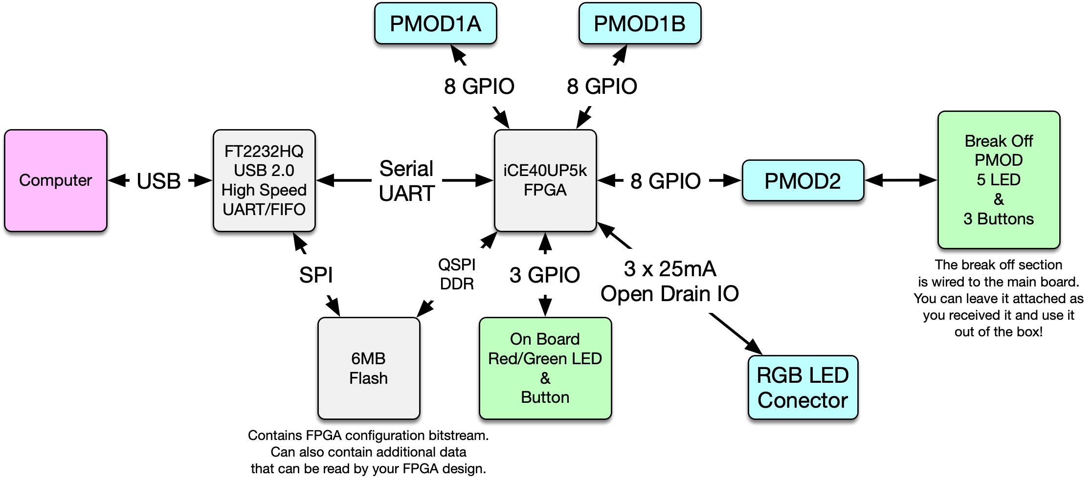
 iCEBreaker block diagram
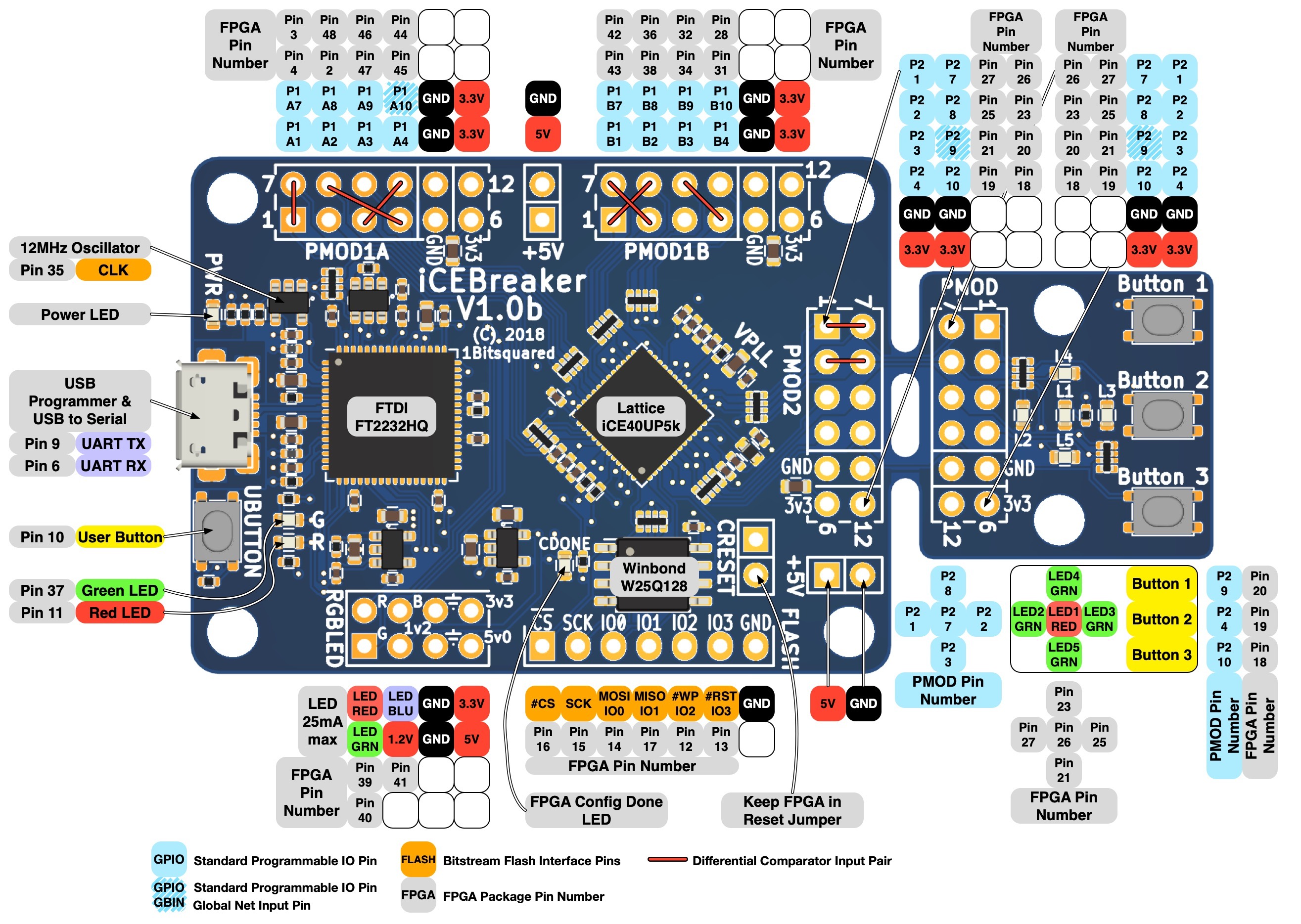
 iCEBreaker V1.0b pinout legend
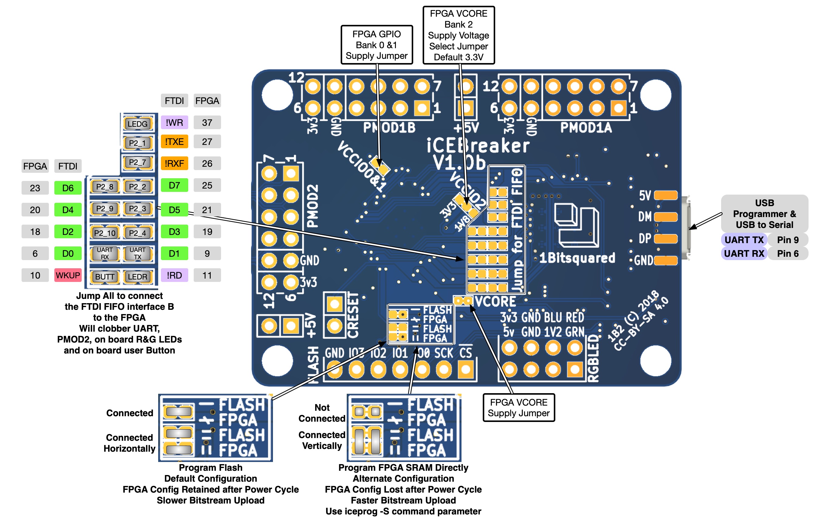
 iCEBreaker V1.0b jumper legend
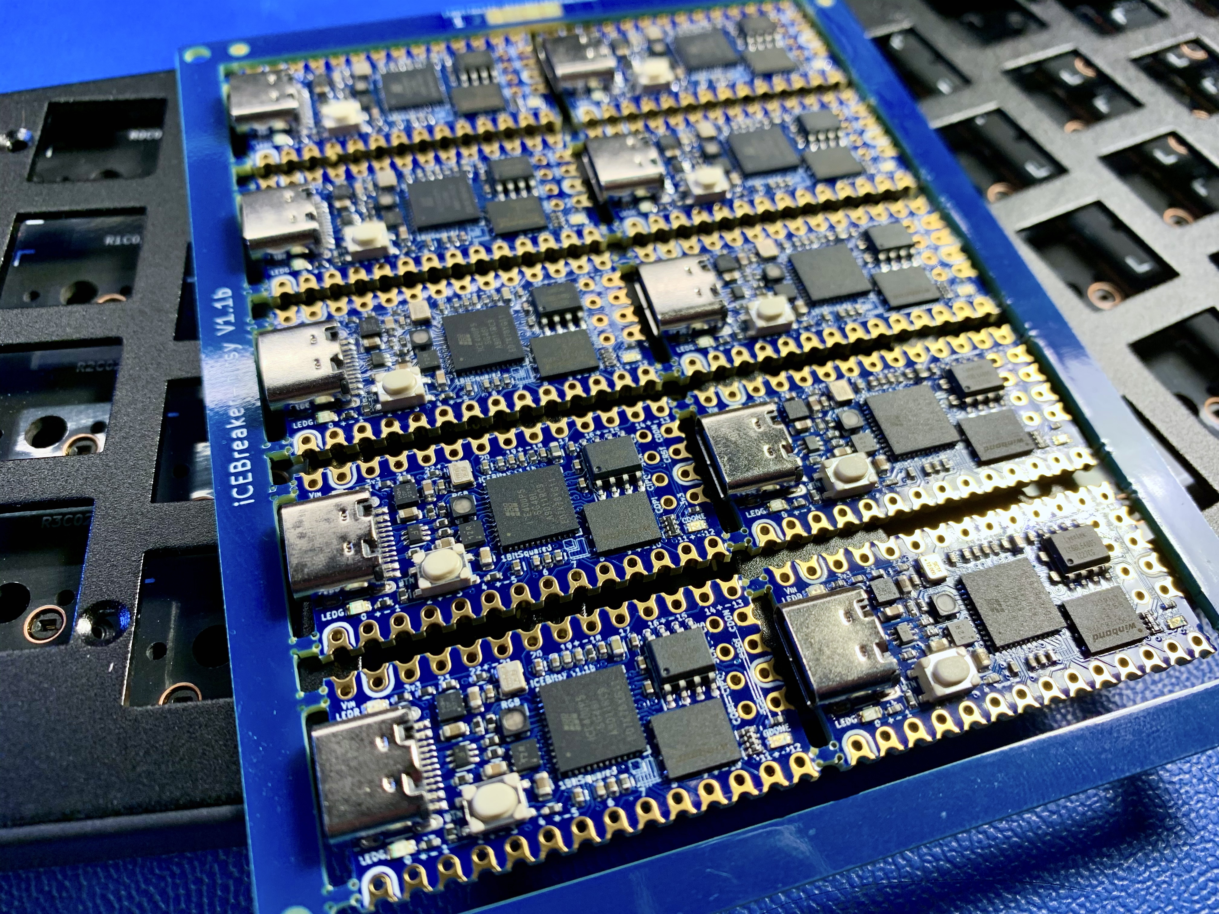
iCEBreaker Bitsy is the smaller but just-as-capable sibling to iCEBreaker. At just 36x18mm, it is compatible with the Teensy form-factor and can be easily embedded into any project.
- iCE40UP5K in QFN48 (SG48) package
- PLL, two SPI and two I2C hard IPs
- 128M (16MiB) DDR- and QPI-capable Flash Memory
- 64M (8MiB) QPI-capable Pseudo-SRAM
- USB-C interface (comes preloaded with a RISC-V soft-core USB bootloader)
- RGB LED connected to 3x 24mA hard PWM IP pins
- Two user LEDs (one shared with RAM-CS)
- Status LED for CDONE (Configuration DONE)
- 12MHz external clock (on PLL GBIN)
- One user button
- Supply rails: 3.3V and 1.2V
- FPGA SPI/programming header
- 4 pins for config (SDI, SDO, SCK, CS)
- 2 extra GPIO pins for QSPI/QPI
- CDONE (Configuration DONE), CRESET (Configuration RESET), 3.3V, and GND
- Teensy form-factor compatible
- Compatible with Feather ecosystem using a Teensy 3.x Feather Adapter
- Castellated edges and single-side-load for easy module integration


