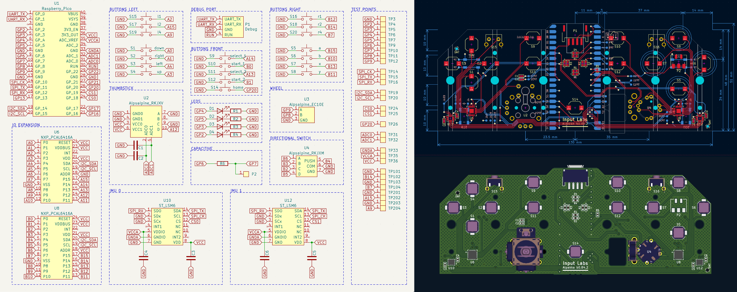
Alpakka controller Printed Circuit Board reference design
- Alpakka Manual.
- Alpakka Firmware.
- Alpakka PCB. (you are here)
- Alpakka 3D-print.
- Input Labs Roadmap.
For ordering a reference design PCB (with no modifications) is possible to use the pre-built order files. Check the manual for step-by-step instructions.
- Open
.kicad_schfile in Schematics editor. - Go to menu
Tools→Edit symbol fields - Group by field
Group - Change id references (
LCSC idfor JLCPCB).
- Copy
plugins/kicad_ilo_export.pyinto KiCad plugins folder (PCB editor → menuTools→External plugins→Reveal plugins folder). - Open
.kicad_pcbfile in PCB editor. - Use menu
Edit→Fill all zones - Go to menu
Tools→External plugins→Refresh plugins - Go to menu
Tools→External plugins→Input Labs: export - Files are generated into
order/
- Open
Preferences→Action plugins - Check that the plugin is installed correctly / check errors.
Consolidated zones increase .kicad_pcb file size significantly, so instead is recommended to load and save the project without consolidation:
- After loading the PCB project:
Edit→Fill all zones. - Before saving the PCB project:
Edit→Unfill all zones.
