MSP430F2013

-
MSP430F20x3家族特色: 具有16-bit sigma-delta A/D converter(差動輸入)
-
16個暫存器
R0 __ program counter R1 __ stack pointer
R2 __ status register
R3 __ constant generator
R4~R15 __ general-purpose registers -
Instruction Set(指令集)
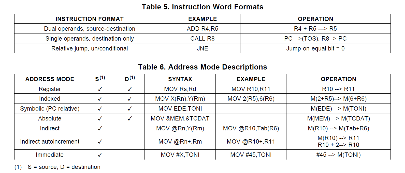
-
Operating Modes MSP430有五種低功耗工作模式。透過中斷可以將設備從五個低功耗模式中喚醒,處理請求並恢復到從中斷程序返回時進入低功耗模式。
• Active mode (AM)
– All clocks are active
• Low-power mode 0 (LPM0)
– CPU is disabled
– ACLK and SMCLK remain active
– MCLK is disabled
• Low-power mode 1 (LPM1)
– CPU is disabled
– ACLK and SMCLK remain active. MCLK is disabled
– DCO's dc-generator is disabled if DCO not used in active mode
• Low-power mode 2 (LPM2)
– CPU is disabled
– MCLK and SMCLK are disabled
– DCO's dc-generator remains enabled
– ACLK remains active
• Low-power mode 3 (LPM3)
– CPU is disabled
– MCLK and SMCLK are disabled
– DCO's dc-generator is disabled
– ACLK remains active
• Low-power mode 4 (LPM4)
– CPU is disabled
– ACLK is disabled
– MCLK and SMCLK are disabled
– DCO's dc-generator is disabled
– Crystal oscillator is stopped -
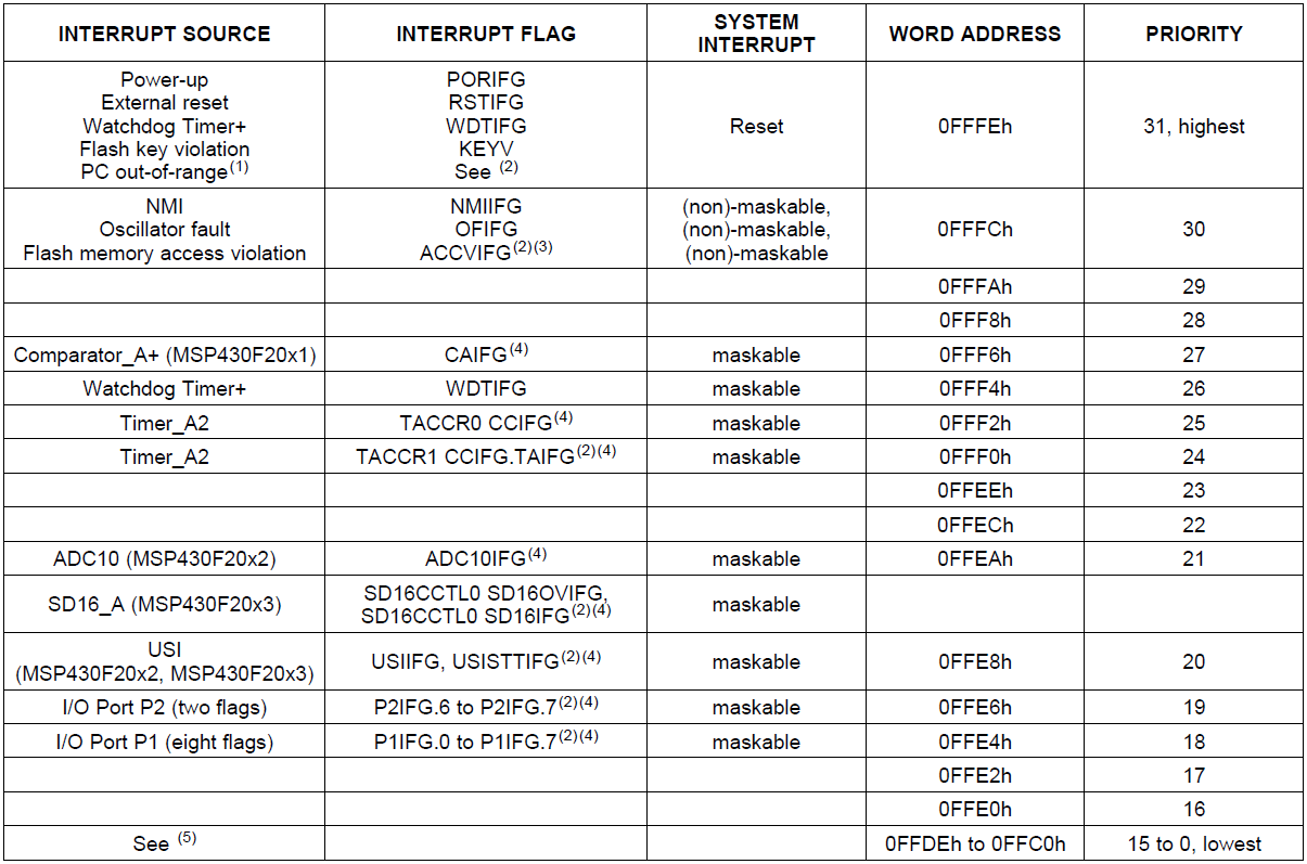
Interrupt Vector Addresses(中斷向量位址) address range of 0FFFFh to 0FFC0h.
-
Special Function Registers:
PUC ("Power Up Clear") 上電清除信號. POR ("Power On Reset") 重置信號.
00h-bit0 WDTIE Watchdog Timer interrupt enable. Inactive if watchdog mode is selected. Active if Watchdog Timer is configured in interval timer mode.
00h-bit1 OFIE Oscillator fault interrupt enable.
00h-bit4 NMIIE (Non)maskable interrupt enable.
00h-bit5 ACCVIE Flash access violation interrupt enable.02h-bit0 WDTIFG Set on watchdog timer overflow (in watchdog mode) or security key violation. Reset on VCC power-on or a reset
condition at the RST/NMI pin in reset mode.
02h-bit1 OFIFG Flag set on oscillator fault.
02h-bit2 PORIFG Power-On Reset interrupt flag. Set on VCC power-up.
02h-bit3 RSTIFG External reset interrupt flag. Set on a reset condition at RST/NMI pin in reset mode. Reset on VCC power-up.
02h-bit4 NMIIFG Set via RST/NMI pin. -
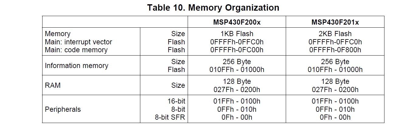
Memory Organization
-
System clock


• Auxiliary clock (ACLK), sourced either from a 32768-Hz watch crystal or the internal LF oscillator.
• Main clock (MCLK), the system clock used by the CPU. 主時脈工廠預設16M
• Sub-Main clock (SMCLK), the sub-system clock used by the peripheral modules.外設用

-
Brownout 掉電保護
The brownout circuit is implemented to provide the proper internal reset signal to the device during power on and power off. -
Digital I/O There is one 8-bit I/O port implemented—port P1—and two bits of I/O port P2:
- All individual I/O bits are independently programmable.
- Any combination of input, output, and interrupt condition is possible.
- Edge-selectable interrupt input capability for all the eight bits of port P1 and the two bits of port P2.
- Read and write access to port-control registers is supported by all instructions.
- Each I/O has an individually programmable pullup or pulldown resistor.
- Watchdog Timer (WDT+)看門狗 主要功能是在以下情況下執行系統重置:
- 出現軟體問題。如果選擇的時間間隔到期,則會生成系統重置。如果看門狗
- 不需要時,可以禁用或將其配置為間隔計時器,並且在選定的時間間隔生成中斷。
IAR embedded workbench
- download: https://www.iar.com/iar-embedded-workbench/#!?architecture=MSP430
- tutorial: https://youtu.be/9QzkK1CaEmM
- visual c++ redistributable: https://support.microsoft.com/zh-tw/help/2977003/the-latest-supported-visual-c-downloads
- User Guides: IAR Embedded Workbench for TI MSP430 https://www.iar.com/support/user-guides/user-guidesiar-embedded-workbench-for-ti-msp430/
JTAG USB debug interface
- MSP-FET
- MSP-FET430UIF

MSP430 USB Stick Development Tool
EZ430-F2013
Flash tools
UniFlash FlashPro-430 and GangPro-430
低雜音長距離 PIR sensor 電路設計與分析

- PIR 之信號應取交流之部分(C2 與 C6),故必須提供1/2Vcc電壓(R2 and R3)。
- OPA開環路增益約為10^5,反饋電路降低整體電路的增益會使系統比較穩定。OPA的開環增益隨頻率快速的下降,限制頻寬(C4,C8)。
- OPA輸出加上RC Filter可以降低OPA輸出之雜音。
- Gain值可能會受到截止頻率之影響。
- Low pass 轉折頻率點設計在10HZ,反推回1/2PI* RC,約1.5K歐姆(R1,R6,R11)
- High pass 轉折頻率點設計在0.7HZ,約1.5K歐姆(R4,R9)
- 直流準位R2=R3=R7=R8=2R4=13.6K歐姆
- Gain 90dB=Gain/2=45dB=177.8*(Vout/Vin),R5 =(Gain-1)* R4 , R5= 1.2M歐姆
- C4,C8 = 1/(2PI * R5 * 10HZ) = 13nF,choose 15nF
焦電型 PIR sensor RE200B 參數與分析

- 受光輻射限制在人體的輻射最敏感的8至14mm範圍。
- JFET S極端子pin2通常通過大約100 K的下拉電阻接地,並放大信號其增益為10,000,在其輸出端產生從0到Vcc的過渡。
- 應將濾波良好的3至15 volts 連接到JFET D極 pin1。Datasheet使用CRC PI型filter。
- 放大器的頻寬通常限制為大約10Hz以阻絕高頻雜訊(1/f)。
- RE200B TO5 package。
- PIR sensor 本體是由一個N通道JFET構成的共汲極放大器(common-drain)
- 根據原理圖,受光面積通過凸透鏡產生更大之角度,而離目標越遠則輸出訊號頻率越低,反之越靠近感測器則頻率越高
- 感測信號強度與距離成反比
- 物體移動速度與頻率成正比,也就是說距離越遠則物體移動越快越容易被偵測到


市售模組 HC-SR505 參數與分析

- Gain = 20 * (3M/10k) = 6000, IC內部有20倍放大OPA輸入
- 實測距離約在2m~3m
- 改動10K為5K後,實測可達3m~4m,再高容易誤報
- 內部PGA倍率越高,則雜訊可承受力越低,當適可而止
- 單端輸入之信號較難以改善從GND涉入之雜訊,理當考慮差動輸入
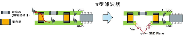
- CRC之PI型濾波,為了避免雜訊直接傳播,可利用Via的寄生電感的手法,經由過孔(Via)與GND平面連接,改善效果較好。
- 有些PCB板佈線佈局,會因串擾而導致濾波效果下降。
- π型濾波器的電容的GND的某些設置方法可能會帶來地線反彈雜訊。
- 優化PCB板佈線佈局可避免這些問題。
- 不要將大容量輸入電容器放置在輸入電源和地之間,而是將其放置在降壓轉換器IC(例如LT1765)的輸入和接地引腳之間。結果是輸出端的電壓紋波明顯降低,電路設計更簡單
