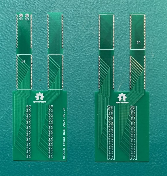
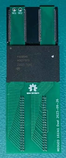
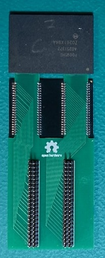
Vortex's VTXCart project allows rewriting the flash/CPLD chips on the 161in1 V3 cart to contain whatever neogeo games you want. However there isn't enough C flash space on a stock 161in1 cart to handle the entire neogeo library.
The C (and V) flash chips come on small daughterboards, one flash chip per daughterboard. This dual daughterboard project is a replacement daughterboard that adds support for 2 flash chips on the daughterboard. This allows increasing the available C flash space from 2G to 3G, which make possible to have the entire neogeo library on the cart.
NOTE: This has only been tested on the MVS version of the 161in1 V3 cart. I have not seen the inside of the AES version to know if the dual daughterboard can fit.
You should select board thickness of 0.8mm.
The board has very fine pitched (0.8mm) castellated holes on it. Ideally you would want to pick the castellated holes option with the PCB manufacture so they get cut cleanly. However the PCB manufacturer will likely reject the order if you pick the option because most require 0.6mm hole diameter and 0.6mm distance between castellated holes.
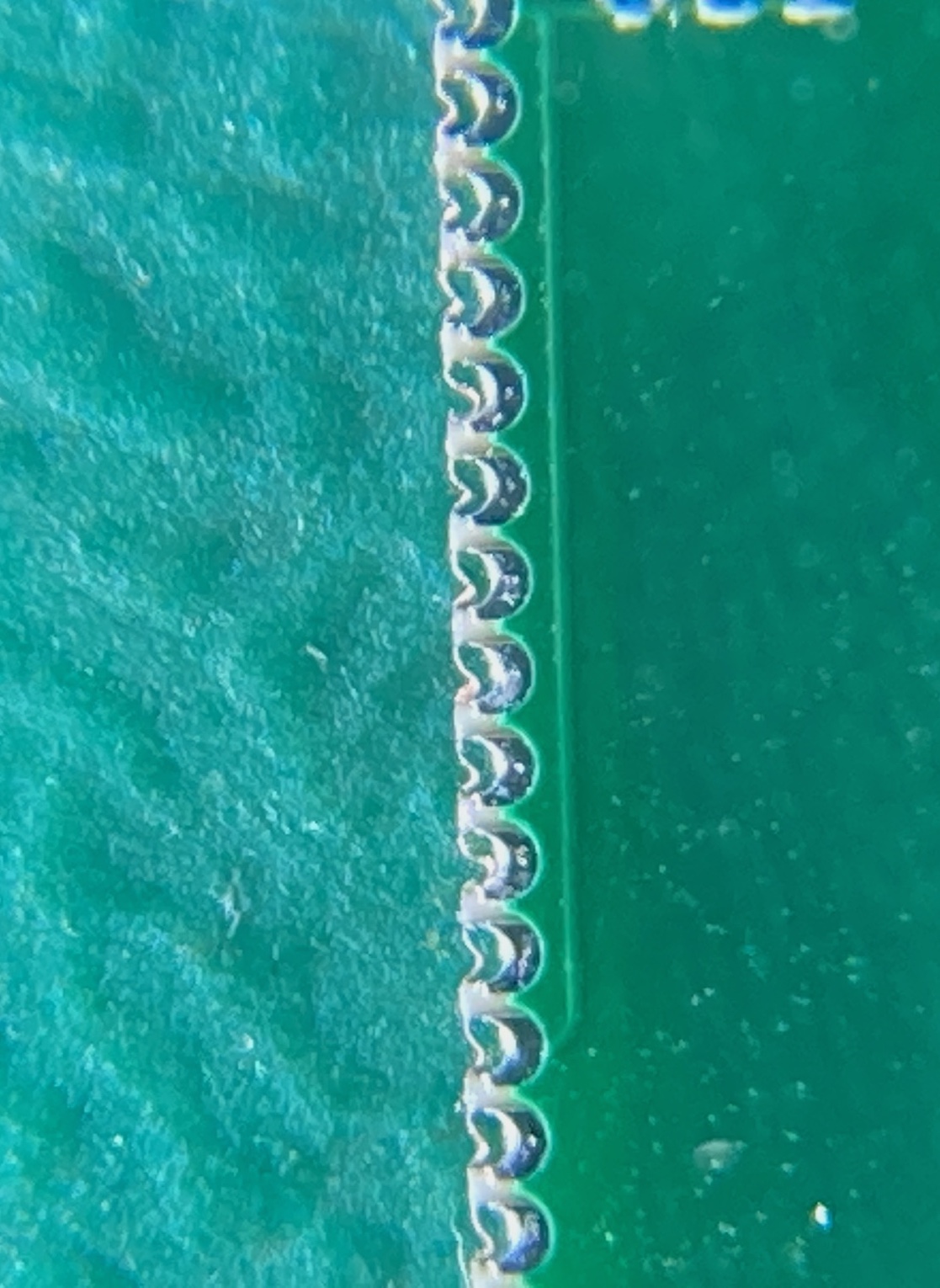
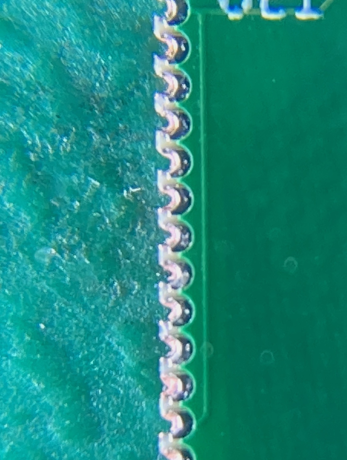
Placing the order without the castellated holes option should go through but will cause the holes to be slightly mangled and look something like this.
You can see how the copper from the left side of the through hole is still there just kinda push flat against the cut path. To fix this you can use fine tipped tweezers to push that extra copper into the right side of the hole. It should end up looking something like this, which is good enough.
Don't attempt to pull the extra copper off or you could rip out all of the copper from the through hole.
Once done, I would suggest using a magnifying glass to verify you see raw pcb between each of the castellated holes.
The 2x F0095H0 flash chips will need to come from a 161in1 board as they don't seem to be something you can just buy.
The dip male connectors are dual row 1.27mm, 22 pins per row, 44 pins total per connector. Best bet is to just by some cheap 2x50 pin connectors and cut them down to size.
I'm going to assume you don't really need soldering advice if you are taking on the task of making a VTXCart. But I will warn you to be careful when soldering the dip connector. It doesn't seem to take much heat and side pressure to cause the individual pins to shift around and you can end up with pins pointing all over the place instead of 2 straight lines.
One thing you need to consider is how you are going to program the flash chips.
With only U1 flash chip installed the dual daughterboard will act the same as a normal daughterboard for reading/writing. So you can use Vortex's F0095H0 dumper board to program it.
However the flash chip that will installed into U2 will need to be flashed by something else. Ideally you should use the original daughterboard it came on with the F0095H0 dumper board.
Running vortex's compiler program with the 'c3g' option will increase the available C rom space to 3G. When completed it should have generated 3 crom files. They need to be flashed as follows.
crom-1 = U1 on dual daughterboard
crom-2 = normal daughterboard (installed in the left most C rom daughterboard location, as seen below)
crom-3 = U2 on dual daughterboard
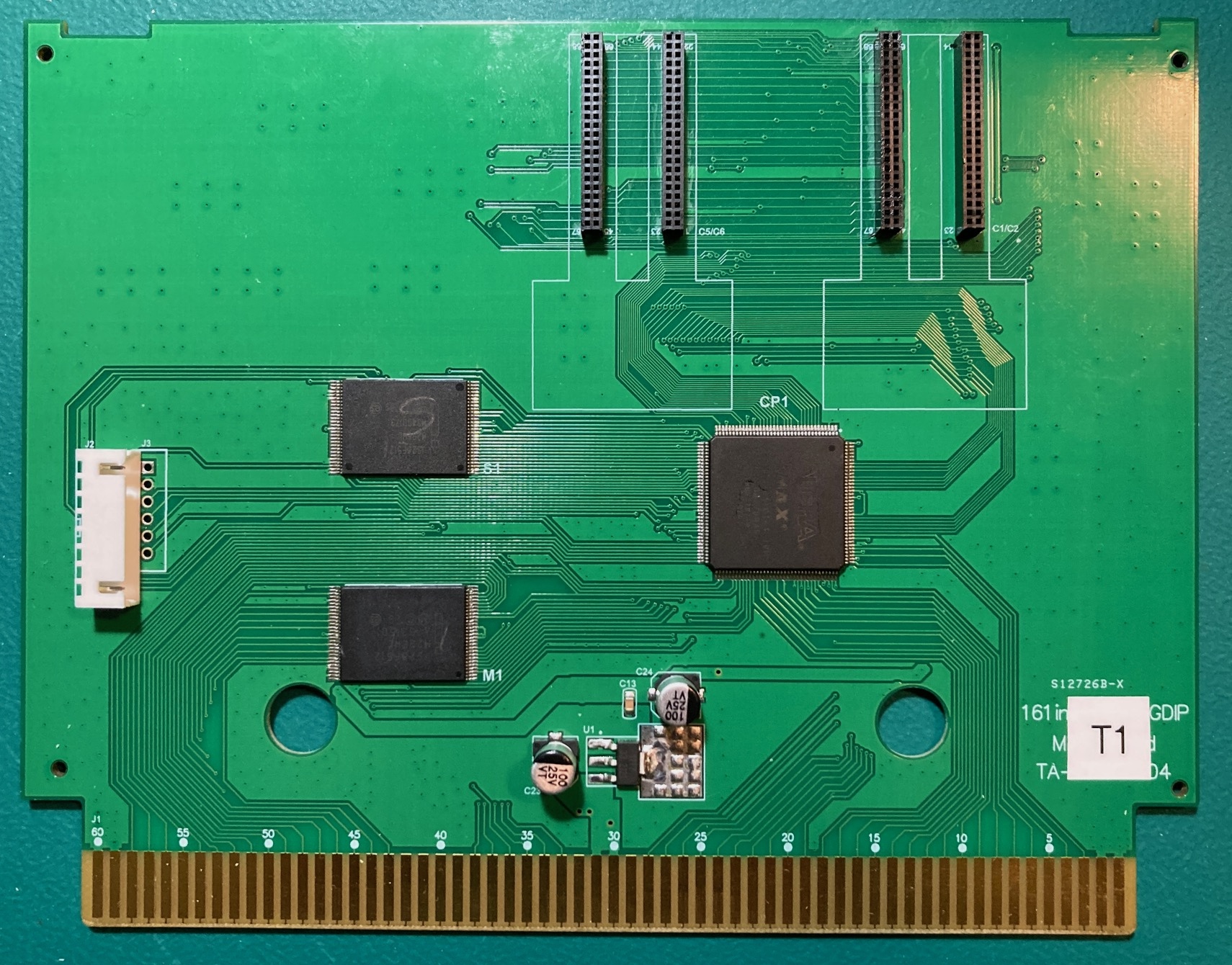
The original daughterboards are soldered to the CHA/PROG boards. As part of creating a VTXCart you should be installing female connectors to make the daughterboards plugable as seen here.
These female connectors are require for the dual daughterboard to fit properly. Trying to solder it directly to the CHA board will cause you to run into clearance issues with the CPLD.
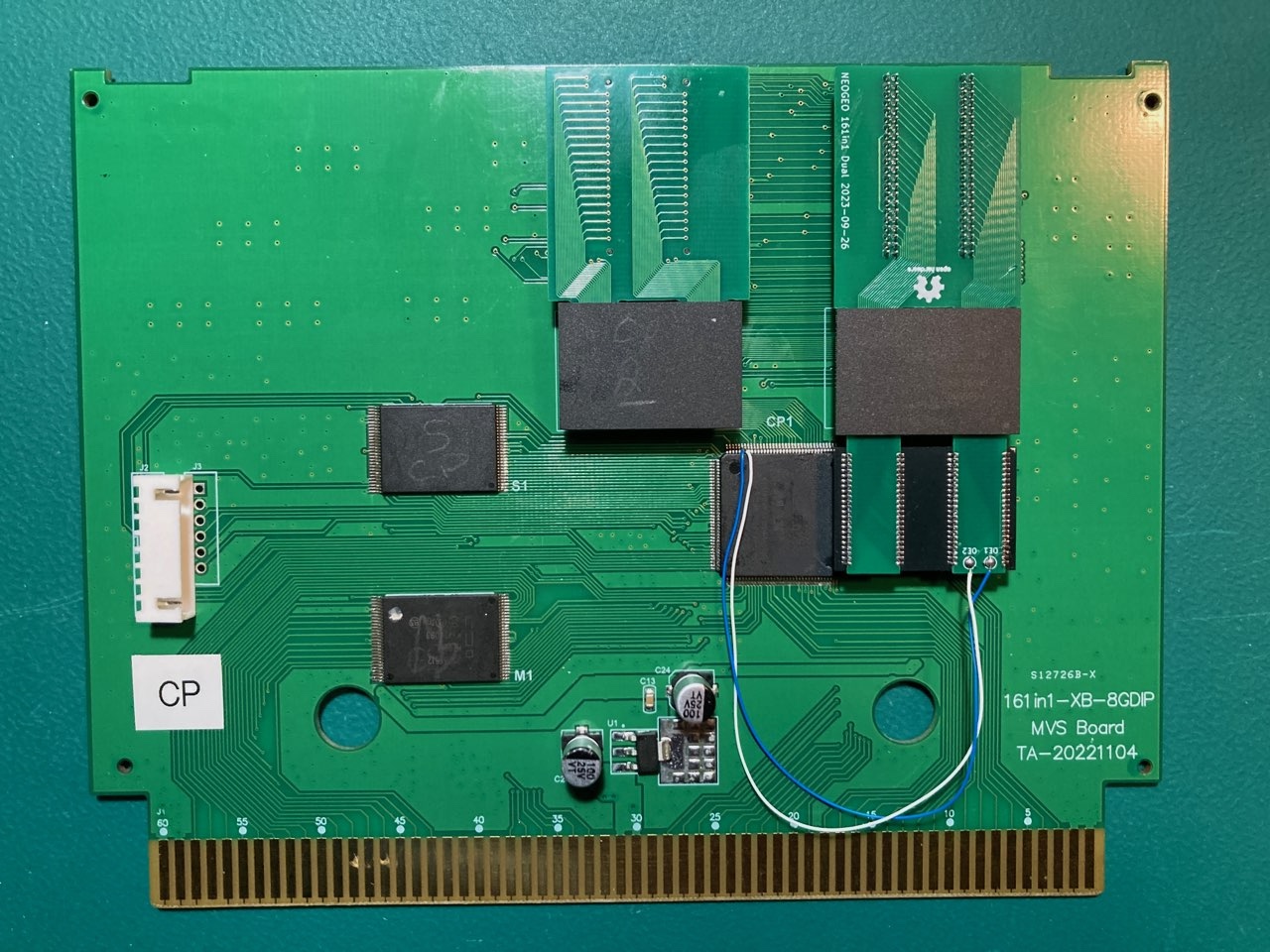
The dual daughterboard must be installed into the right most C rom daughterboard location. Its not possible for it to be installed in the left location because it would collide with the white board to board connector on the back of the PROG board. This is also why you can't do 4G of C rom space (not that there would be a need to have that much).
The OE1 and OE2 pins on the dual daughterboard need to be soldered to pins on the CPLD. As of right now the allocated pins are
AES:
- OE1 = PIN 48
- OE2 = PIN 47
MVS
- OE1 = PIN 31
- OE2 = PIN 30
You should however verify this is still the case by looking at the pin assignments for the CHA_CP1 CPLD in the VTXCart project. Look for C3_nOE[0] (OE1) and C3_nOE[1] (OE2) under Assignments -> Pin Planner in Quartus.
Fully installed it should looks like this (MVS)
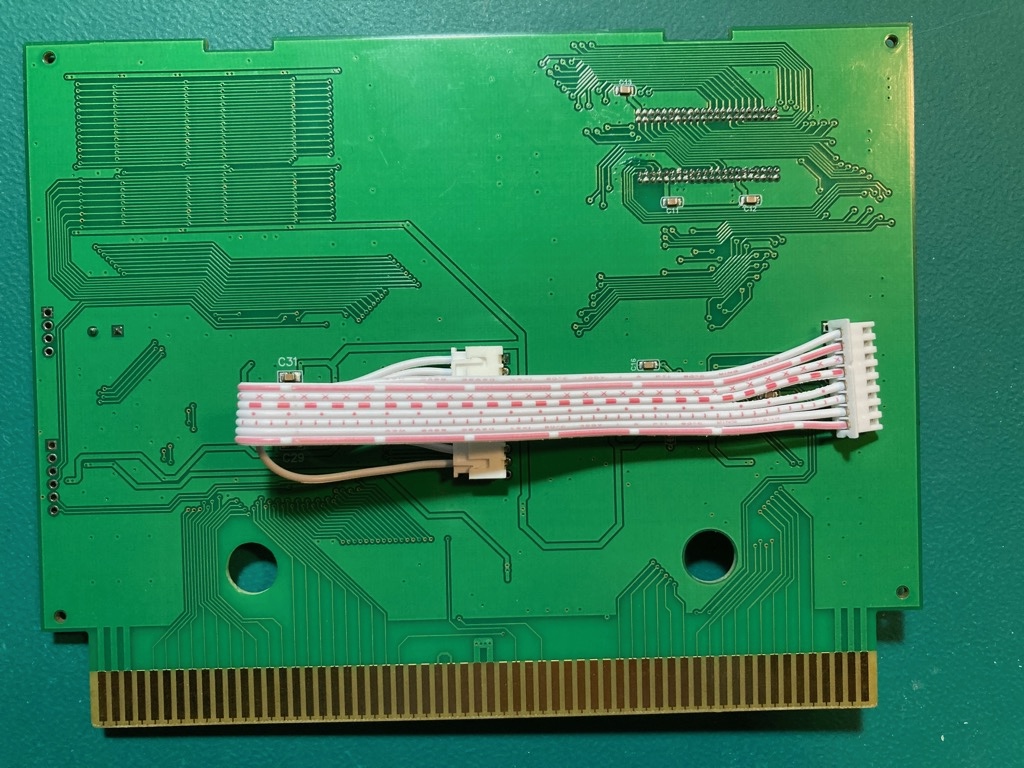
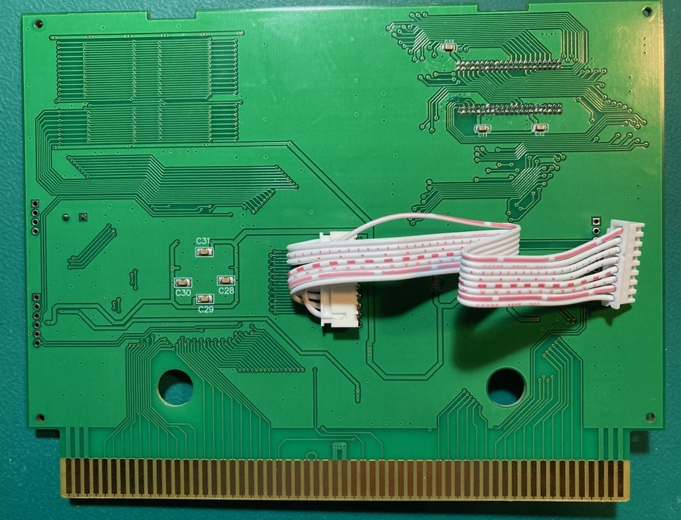
Lastly an adjustment needs to be made to the bends of board the board cable to make space for the dual daughterboard.
