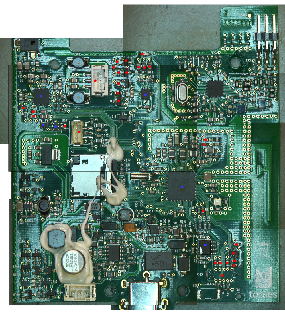
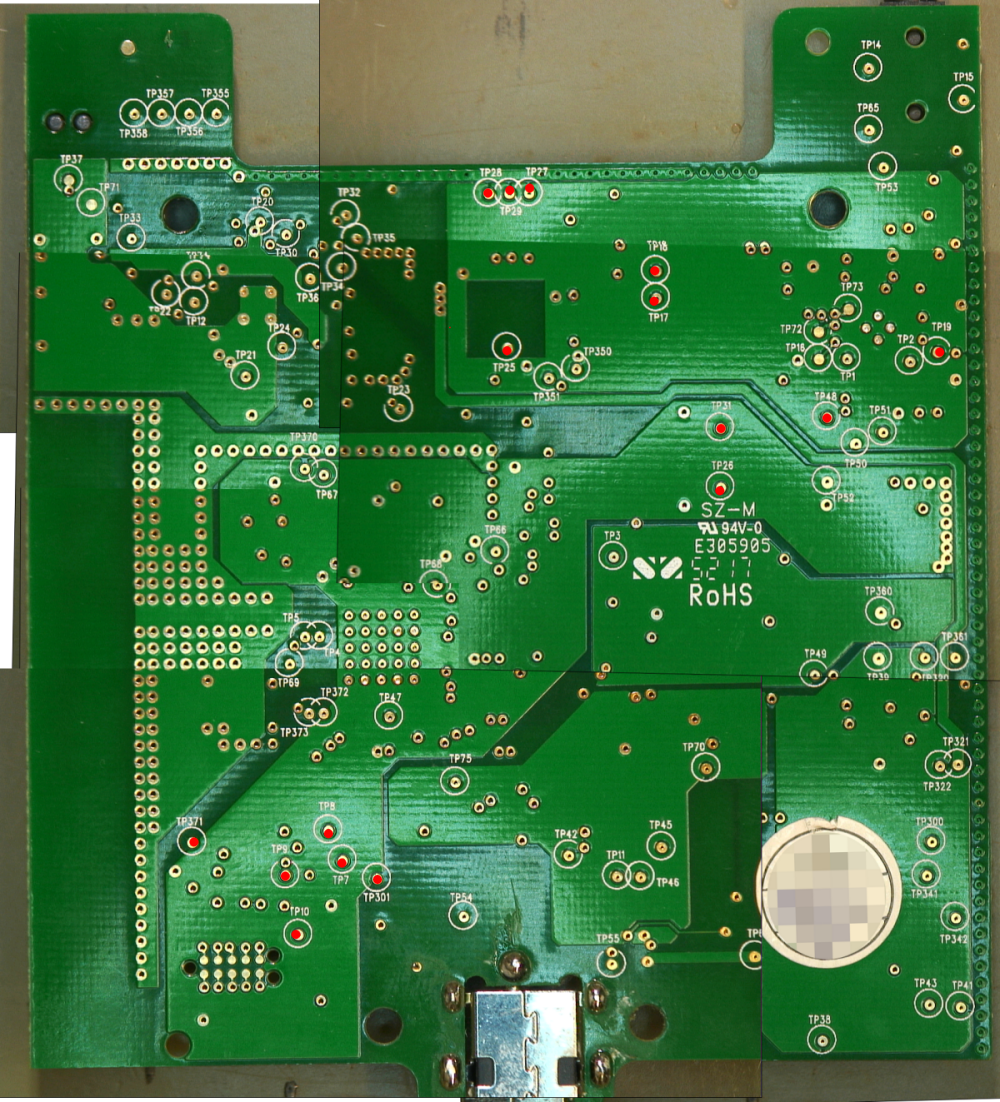
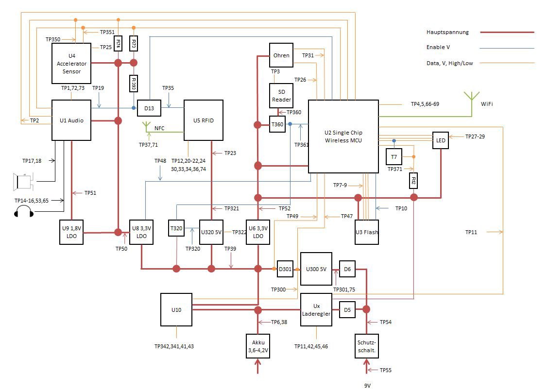
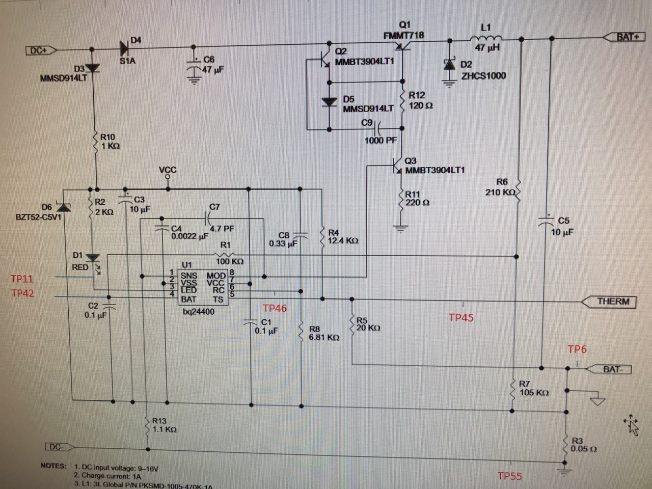
Repository which will lead to a complete schematic of a Toniebox PCB. The schematic is done with KiCad.
View this project on CADLAB.io.
Source of CC3200 footprint: https://raw.githubusercontent.com/Turegano/CC3200/master/lib/CC3200.lib
- datasheets
- doc: documentation
- library: KiCad libraries
- red dot: fully documented
- blue dot: partially documented
-
create subsheets for logical blocks
-
create pinout of ASICs
-
document remaining testpoints
T1: NSS40200LTG
| TP | Connected to | Comment |
|---|---|---|
| TP1 | U1 MCLK | external master clock |
| TP2 | U1 GPIO1/ U2 pin 55 GPIO1 | |
| TP3 | K2 pin 9 | SD detect |
| TP4 | U2 pin 29 | ANT SEL1 Antenna Selection Control |
| TP5 | U2 pin 30 | ANT SEL2 Antenna Selection Control |
| TP6 | BQ24400 GND/Battery GND | Battery GND is connected with PCB GND via R55 (0R05) |
| TP7 | U2 pin 11/U3 pin 6/R27(?) | SCK |
| TP8 | U2 pin 12/U3 pin 5/R26(?) | SI |
| TP9 | U2 pin 13/U3 pin 2/R25(?) | SO |
| TP10 | U2 pin 14/U3 pin 8/R28(?) | VCC |
| TP11 | U7 pin 3 (~LED) | Charge status LED, connected to U6 output via 100k pull up and U2 pin 20 via 1k2 |
| TP12 | U5 ASK/OOK | can be configured as an output to provide the received analog signal output |
| TP14 | audio jack | |
| TP15 | audio jack | |
| TP16 | U1 VOL/MICDETECT | |
| TP17 | K9 pin 3/U1 | speaker+ |
| TP18 | K9 pin 2/U1 | speaker- |
| TP19 | U1 pin 31/D12/U2 pin 62 GPIO7/U5 EN | DAC reset |
| TP20 | U5 VDD_X | |
| TP21 | U5 VDD | |
| TP22 | U5 BG | |
| TP23 | U5 VIN | Voltage of U320, if faulty check TP321 |
| TP24 | U5 VDD_A | |
| TP25 | U4 pin 3 | Accelerometer DNC |
| TP26 | K4 pin 1/U2 pin 57/R60 (1k)(?)/R394 (1k2)(?)/ | ears, fed from regulator U6/TP52 |
| TP27 | D10 pin 1 | LED red - |
| TP28 | D10 pin 2 | LED green - |
| TP29 | D10 pin 3 | LED blue - |
| TP30 | U5 IO 5 | |
| TP31 | K4 pin 3/U2 pin 59/R64(1k)(?) | ears, fed from regulator U6/TP52 |
| TP32 | ||
| TP33 | U5 MOD | |
| TP34 | U5 SYS | |
| TP35 | U5 EN | When high NFC IC is enabled. If faulty check TP19. Fed by U8 via D13 (is connected to U2 GPIO7). |
| TP36 | U5 EN2 | |
| TP37 | NFC socket | |
| TP38 | K8 pin 3/T1/D12 (battery control circuit)/T340/T342 | bat+ |
| TP39 | U320 VIN, T320 collector voltage for U320 EN via R320; U6 VIN; U8 VIN | feeds U320, U6, U8 with VCC; enables U320 via T320 |
| TP41 | Circuit next to U10 | 0V w/o battery, ~ bat. Voltage w/ battery; output of T344; connected to U10; controls T343, T342, T340 |
| TP42 | BQ24400 BAT input | |
| TP43 | U10 / | battery voltage after R89; w/ battery: voltage < bat voltage; w/ power supply 3.8 – 4.4V; check TP38 if not ok |
| TP45 | K8 pin 1/U7 pin 5 (TS) | temp sense; connected via R47 with BQ24400 and battery NTC. |
| TP46 | BQ24400 TIMER PROGRAM | |
| TP47 | U2 pin 8/output L300 via 1:1 voltage divider R75/R72 | Supervising U300+circuitry; measured between D301 and L300; 50% voltage via divider R75/R72 to U2 pin 8 |
| TP48 | U2 pin 61/U8 ENABLE via R56 (10k pulldown) | U2 enables LDO U8 with GPIO6. If U8 is not working (TP50) check U8 at TP39 |
| TP49 | U2 pin 60 | |
| TP50 | U8 VOUT/U9 VIN/U1 IOVDD/U1 HPVDD/SPKVDD/AVDD | 3V3 output of LDO U8, 1V8 input of LDO U9, T11, U4. 3V3 input U1; if not ok check TP48. |
| TP51 | U9 VOUT/U1 DVDP | 1V8 output of LDO U9. Feeds U1 at PIN 3; if not ok check ENABLE at TP50 and input voltage at TP39. |
| TP52 | U6 VOUT 3V3/ U2 VIN IO1, VIN IO2, VIN DCDC ANA, VIN DCDC PA, VIN DCDC DIG, VD2 ANA2/ VCC for U3,T7, T360, T320, SV BQ24400 LED/ RGB LED | 3V3 output LDO U6: feeds U2, U3, T360 (TP360), TP320, LED output of BQ24400 (TP11) |
| TP53 | audio jack | |
| TP54 | VCC | Power supply voltage; if power supply is ok check L8 (SMT Common Mode Line Filter 2x500mH) and D4 (15V TVS Diode) |
| TP55 | GND power jack | |
| TP65 | audio jack | |
| TP66 | U2 pin 43/pin 9/pin 56 | U2 internal voltage |
| TP67 | U2 pin 38/pin 36/pin 48/pin 25 | U2 internal voltage |
| TP68 | U2 pin 48 | U2 internal voltage |
| TP69 | U2 pin 24 | U2 internal voltage |
| TP70 | T9 | middle pin (SMD 13014) |
| TP71 | U5 VSS PA/VSS RF/VSS/VSS D/NFC connector outer contacts | |
| TP72 | U1 AIN1 | |
| TP73 | U1 AIN2 | |
| TP74 | U5 IRQ | |
| TP75 | U300 VIN | comes from R305 (0R). U300 generates voltage when operating with power supply; if not ok check TP301 |
| TP300 | U300 ISENS/T347 via R344 | U300 output voltage; main supply when connected to power supply; input voltage of voltage divider R344/R345 for U10. |
| TP301 | D6 | Main voltage after D6;if not ok check TP54 |
| TP320 | U320 ENABLE/T320 | ENABLE U320 from T320; T320 is supplied via R320 (470k) from D301 (TP39); T320 is controlled by U2 pin 58; if not ok check TP361 and supply voltage of TP39 |
| TP321 | U320 output/U5 input | U320 supplies U5; if not ok check TP320 and TP39 for supply voltage; if supply voltage check TP322 |
| TP322 | U320 feedback | Voltage for regulating output voltage of U320; output voltage of divider R321 (470k)/R322 (180k); should be 1.31V-1.51V; divider is fed by U320 output; if not ok check output TP321, input TP39, ENABLE TP320 |
| TP341 | U10 circuitry | ;output of T347; controls T346, T345, T341; LOW when operating with power supply; ~ bat voltage when operating with battery; check TP342 and TP38 |
| TP342 | U10 circuitry/voltage divider R344/R345 | Voltage divider R344/R345; fed from output of U300; triggers T344, T347 getriggert; operating with power supply: 1V; battery mode: 0V;check TP300 |
| TP350 | U2 pin 3 | I2C_SCL |
| TP351 | U2 pin 4 | I2C_SDA |
| TP355 | config(?) R connected to GND | |
| TP356 | config(?) R connected to GND | |
| TP357 | config(?) R connected to GND | |
| TP358 | config(?) R connected to GND | |
| TP360 | K2 pin4 | SD VDD;T360 switches 3V3 of U6; T360 is controlled by U2 GPIO3 PIN58; check TP361 |
| TP361 | T320/T360 (voltage) | T320 switches ENABLE of U320 / T360 controls voltage SD card |
| TP370 | U2 pin 34 SOP1 | |
| TP371 | U2 pin 35 SOP0 | |
| TP372 | U2 pin 17 TDO | |
| TP373 | U2 pin 18 |


