SPLA: Super Nintendo PPU Logic Analyzer
The 1990-era Super Nintendo Entertainment System is a venerable gaming console, and although its hardware is aging and hard to come by, it has long had well-establish software emulators, preserving gaming history for generations to come.
However, while most of the SNES hardware has been effectively
reverse-engineered by writing test programs for the CPU (sometimes taking
advantage of undocumented behavior to figure out details), one remaining
component of the console has resisted complete analysis: the "Picture
Processing Unit" chips, PPU-1 and PPU-2.
The PPU chips are together responsible for managing the sprites, backgrounds, and palettes for each frame of a game's video output, and produce the analog scanline signal in realtime, which then appears on the player's TV. However, the output video signals (and video ram bus) are entirely inaccessible to SNES CPU, thus making analysis of the exact timing details of these chips difficult or impossible.
A very few games for the SNES (particularly Air Strike Patrol) use the SNES video hardware in unexpected ways, which depend on the detailed timing of the PPU chips during scanline rendering. This makes accurately emulating these games' graphics difficult -- emulator developers have to manually compare emulator output with what the game actually shows on the screen, and try to guess how the PPU evaluates these unusual configurations. Without complete understanding of the chips operation, this process degenerates into a frustruating game of whack-a-mole.
To be confident that we have faithfully reproduced the entire SNES, we need to characterize all the PPU outputs at the level of individual clock cycles, and rigorously compare the behavior of a software emulator to that of the actual, physical chips.
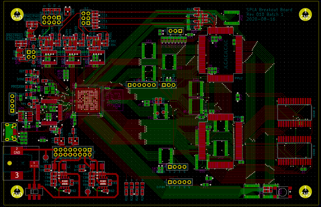
This project is intended to design a breakout circuit board, integrating the SNES PPU chips from a real vintage SNES console, combined with surrounding modern hardware, to effectively form a >100-pin-wide digital logic analyzer, combined with single-frame analog video capture system. With this board built, and sufficient supporting software written, it should be possible to experimentally characterize the entire operation of the PPU chips, thus producing a completely cycle-accurate emulation of the SNES video hardware.
Current Status
- Design complete.
- Schematic complete.
- PCB layout complete.
- Schematic and PCB review complete (enough).
- Lab setup essentially complete.
- Bringup started.
- Power bringup complete.
- USB / FTDI bringup complete.
- FPGA bringup complete.
- Level shifter bringup complete.
- SNES bringup complete.
- Analog bringup pending.
- Software development in progress.
- Early bringup and testing software complete.
- RTL development in progress.
- All bringup images complete.
- Low-speed driver image in progress.
- High-speed driver image pending.
Design components
- The USB interface to a host PC is based on an FTDI
FT2232Hchip, which can drive up to 60MBps (USB 2.0 "Full Speed" maximum throughput). - A Lattice
ECP5FPGA, which forms the central brains of the board. - Both SNES
PPUchips, and their corresponding video SRAM chips (which are standard 32KiB 8-bit SRAM chips, but are old enough that they're hard to source). - A whole bunch of 3.3V / 5V level shifter chips (
74LVC8T245), as the SNES chips are 5V TTL, but almost everything modern is 3.3V at most. - Three
ADC1173high-speed 8-bit analog-to-digital converter chips, to capture the analog RGB signal output and convert it back to digital for analysis. This also requires a handful (5) ofLMH6611opamps to drive the ADC inputs and establish reliable references.
