Memory Testing Module Tutorial
Experimental results available online for easy viewing at: https://drive.google.com/open?id=1uQApV60ZPeULmpTdM61_w9c1aRNkuKza
Backup results available in this git in the "Experiment Results FPT2019" folder. Downloaded results can be viewed using Microsoft Excel or any compatible software.
The tabs finishing in "-C" hold only charts generated by the data obtained using the particular configuration. Most charts have repetitive data/uninteresting trends, but they were all generated, to observe (if) any unexpected results have occured.
The provided module contains other IPs provided by Xilinx to instantiate some primitives such as BlockRams.
To hide all this and easiest usage, the memory testing module is packaged as an IP.
This IP is located in the "IP" folder and once added to a Vivado project, can be instantiated as any other IP in the Xilinx Vivado toolchain. This IP is packaged using Vivado 18.2.1.
The module's interface is made up by 1 clock, 1 low active reset, 1 Master AXI interface that needs to be connected to a DDR AXI port, and 1 Slave AXI port which is used by software to control the test execution and obtain the PMU results.
The example driver provided (IP/Driver Example/helloworld.c) shows the needed information to run the tests. The sequence is: 1) Reset 2) Configure 3) Start 4) Sleep 5) Stop 6) Wait for the stop 7) Read PMU out. For each of these steps, functions have been provided. Noting: Configuring is separate for the read and write ports of the master AXI. After commanding the accelerators to stop, they stop issuing new memory requests and wait (keep counting including runtime) until all of the on-flight operations are executed. This is why a function is provided to wait for the accelerators to fully finish execution.
- Open Vivado 2018.2.1 and create a new project.
- Create Block Design
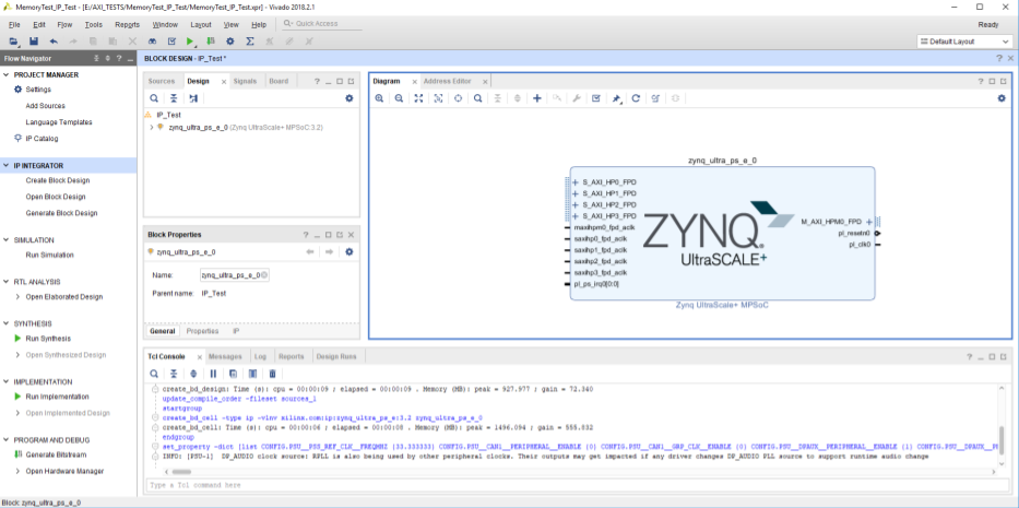
- Instantiate Zynq Ultrascale+ MPSoC
- Configure Zynq UltraScale+ MPSoC according to the used board and:
- Add one or multiple HP AXI ports to be tested.
- Add one master AXI port - AXI HPM0 FPD.
- Configure desired DDR organisation.
- Configure desired clock frequency.
Example state of the project so far:

- Download “MemoryTestBlock.zip” and unzip it.
- In Vivado, open Tools->Settings->IP->Repository->Add, and navigate to the folder with the unzipped contents.
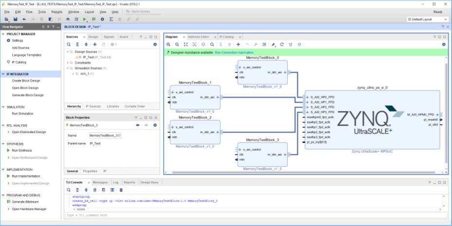
- In your block design, add a new IP called “MemoryTestBlock”. Add it as many times as AXI HP ports used.
- Connect manually the “m_ddr_axi” ports on the module to the AXI HP ports either directly or with interconnect:

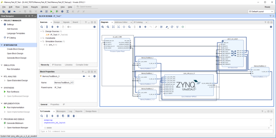
- Now “Run Connection Automation” and select everything listed. Vivado will connect automatically the clock sources, reset signals and the slave AXIs:

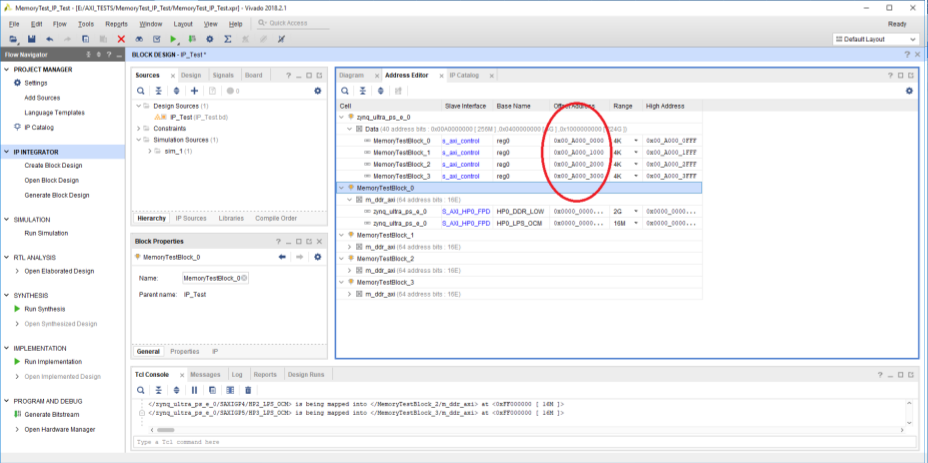
- In the “Address Editor”, you now have to assign all the DDR memory space to all accelerators. Additionally, you have to remember which HP AXI port is connected to which MemoryTestBlock and the corresponding global address of the slave port. In our case HP0 is connected to MemoryTestBlock_0 and mapped to 0xA000_0000. Thus the control port for HP0 is at 0xA000_0000:

- Save and Validate your block design. Right-click on it and select “Create HDL Wrapper”.
- Make sure the created wrapper is the design’s top module and then synthesize, implement and generate bitstream.
- Export the hardware by File->Export->Export Hardware. Tick “Include Bitstream”.
- Start SDK by File->Launch SDK.
- In SDK create a new “Hello World” application project. Use the exported hardware and generate a new BSP.
- Allocate most of the available DDR memory in the heap in the linker file (lscript.ld).
- Copy the example driver source code (IP/Driver Example/helloworld.c) in your main C file.
- Modify the slave addresses of the memory test modules to match the assigning from step 10. They are represented as variables HP0, HP1, HP2, and HP3 in the source code.
- Compile and upload on an FPGA.