COMP2270: Computer Architecture
|
Note
|
The class midterm is coming on October 2. |
September 1
Introduce yourself
Welcome! Let’s get to know each other with an icebreaker. Answer these questions:
-
What is your name?
-
Why is Computer Science your major?
-
Tell us something nobody else in the room knows about you.
About this course
This course introduces digital logic, combinational and sequential circuit design, and computer architecture (hence the name).
We’ll have a midterm, labs and assignments, but for the final project, we’ll design, implement and test a CPU in a simulator.
The textbook is recommended, but not required. Let’s use free books, instead:
September 3
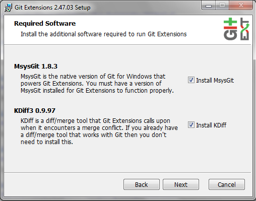
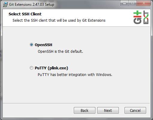
Install Git and frontends
- Windows
-
Note
Select KDiff, and choose OpenSSH (not PuTTY); otherwise, stick to the default settings. - Mac OS X
- Linux
-
Install git using your package manager.
NoteDon’t forget to use sudo with your package manager.
Run starterupper
Starterupper sets up git and project hosting for this class; it is safe to run even if you already have git and SSH keys set up on your machine.
Open Git Bash (Windows) or Terminal (Linux, Mac OS X) and paste in the command below.
Press Shift-Insert to paste in Git Bash.
curl https://gitlab.com/lawrancej/COMP2270-2015/raw/master/main.sh | bash
Intermission
Short break.
Number bases

The base or radix is the number of digits used to represent a number.
| Base | Name | Base label | Digits | Example |
|---|---|---|---|---|
2 |
Binary |
0b |
0-1 |
0b1010 |
8 |
Octal |
0o |
0-7 |
0o12 |
10 |
Decimal |
None |
0-9 |
10 |
16 |
Hexadecimal |
0x |
0-9,A-F |
0xA |
Each number base has a Latin root shared with other words. Bi means two, as in binary, bicycle, bisexual. Oct means eight, as in octal, octagon (stop sign) and October. Deci means ten, as in decimal, December and decimate. Hex means six, as in hexadecimal (think 6 + 10) and hexagon. Fun fact: October and December were the eighth and tenth month before Julius and Augustus Caesar named months after themselves. Fun fact: decimate meant killing every tenth soldier for group punishment (those Romans!).
Assume numbers without a prefix are in decimal, unless prefixed with a base label. A base label identifies the number base (e.g., 0b, 0o, 0x). Thus, 1011.1 means one thousand eleven and one tenth, but 0b1011.1 means 11.5 in decimal.
Number base uses
Binary works reliably everywhere.
| Binary | Number | 0 | 1 |
|---|---|---|---|
Boolean |
Value |
False |
True |
English |
Word |
No |
Yes |
Switch |
Position |
Off |
On |
CPU |
Voltage |
Low |
High |
HD |
Magnetic Polarity |
South |
North |
CD-ROM |
Pit/land edge |
Non-edge |
Edge |
RAM |
Electric charge |
Negative |
Positive |
Finger |
Position |
Closed |
Extended |
Octal is used in Linux/Unix to represent read/write/execute permissions for users, groups, and others.
Hexadecimal is a compact number representation that is found in IPv6 addresses, SHA hashes, and so forth.
Digits and place values
Each digit in a number has a place value. The place values in any number base are powers of the base.
Example: Decimal number 278.1 has four digits and place values (and a decimal point). We read this number as two hundred seven ty eight and one tenth. That is, 278.1 is 2 * 100 + 7 * 10 + 8 * 1 + 1 * 0.1.
| Place value | hundreds (10^2) | tens (10^1) | ones (10^0) | decimal point | tenths (10^-1) |
|---|---|---|---|---|---|
Digit |
2 |
7 |
8 |
. |
1 |
Example: Binary number 0b1011.1 has five bits (binary digits) and place values. Read this as "binary number one zero one one point one". That is, 0b1011.1 is 8 * 1 + 4 * 0 + 1 * 2 + 1 * 1 + 1 * 0.5, or more simply 8 + 2 + 1 + 0.5 = 11.5 in decimal.
| Place value | 8 (2^3) | 4 (2^2) | 2 (2^1) | 1 (2^0) | radix point | 0.5 (2^-1) |
|---|---|---|---|---|---|---|
Bit |
1 |
0 |
1 |
1 |
. |
1 |
|
Note
|
DO NOT read decimal place values for other number bases. For example, do not read 0b1011.1 as "one thousand eleven and one tenth", because that implies a decimal number. |
Counting
|
Note
|
The first digit in a number (on the left) is the most significant; the last digit (on the right) least significant. Zeroes on the left don’t affect the number. |
To count in any number base, picture an odometer: the least significant digit cycles faster than the most significant digit while counting.
-
Write out all desired place values
-
Writing from top to bottom, not left to right, cycle through all digits, repeating each digit as many times as indicated by the corresponding place value above.
Example: Counting nibbles, single hex digits, two-digit octal and two-digit decimal.
| Binary | Hexadecimal | Octal | Decimal |
|---|---|---|---|
0000 |
0 |
00 |
00 |
0001 |
1 |
01 |
01 |
0010 |
2 |
02 |
02 |
0011 |
3 |
03 |
03 |
0100 |
4 |
04 |
04 |
0101 |
5 |
05 |
05 |
0110 |
6 |
06 |
06 |
0111 |
7 |
07 |
07 |
1000 |
8 |
10 |
08 |
1001 |
9 |
11 |
09 |
1010 |
A |
12 |
10 |
1011 |
B |
13 |
11 |
1100 |
C |
14 |
12 |
1101 |
D |
15 |
13 |
1110 |
E |
16 |
14 |
1111 |
F |
17 |
15 |
Notice the pattern of cycling (and repetition) through digits in each number base? Binary cycles between 0 and 1 under the least significant place value, and in the 2’s place, it cycles between 00 and 11, and so forth.
Challenge: What will the next row in the table above look like?
|
Note
|
10 in any base means the base itself. Think about why. What’s 0b10 in decimal? How’d you know that? |
Binary → decimal
To convert from binary to decimal,
-
Write out place values (powers of two) above each binary digit (bit)
-
Add up place values when the corresponding bit is 1
Example: What is 0b111100 in decimal?
| Place value | 32 (2^5) | 16 (2^4) | 8 (2^3) | 4 (2^2) | 2 (2^1) | 1 (2^0) |
|---|---|---|---|---|---|---|
Bit |
1 |
1 |
1 |
1 |
0 |
0 |
It is 32 + 16 + 8 + 4 = 60.
Challenge: What is 0b1101101 in decimal?
Decimal → binary
To convert from decimal to binary,
-
Find the highest power of two less than or equal to the number
-
Write out all place values (powers of two) up to the number found in step 1
-
Make change with powers of two (repeat step 1)
Example: Convert 278.1 to binary. 256 is the highest power of two less than 278.1, so subtract away, and repeat.
    278.1
  - 256    (2^8)
  --------
     22.1
   - 16    (2^4)
   -------
      6.1
    - 4    (2^2)
    ------
      2.1
    - 2    (2^1)
    ------
      0.1
    - 0.0625 (2^-4)
    --------
      0.0375
    - 0.03125 (2^-5)
    ---------
      0.00625
      ... and so forth...
At this point, to write out the binary number, just place a 1 corresponding to each place value we subtracted away, and zero elsewhere.
| Place value | 256 | 128 | 64 | 32 | 16 | 8 | 4 | 2 | 1 | Radix point | 0.5 | 0.25 | 0.125 | 0.0625 | 0.03125 |
|---|---|---|---|---|---|---|---|---|---|---|---|---|---|---|---|
Bit |
1 |
0 |
0 |
0 |
1 |
0 |
1 |
1 |
0 |
. |
0 |
0 |
0 |
1 |
1 |
Fractions
You may think: "Hey, we’re not done yet!" You’re right, the binary number above is not exactly 278.1 in decimal, but it is worth noting that some fractional numbers cannot be represented exactly. For example, 1/3 in decimal is 0.3333…. We cannot represent that number in decimal, and decimal numbers such as 0.65 cannot be represented exactly in binary. This is why we care about precision when dealing with floating point numbers, and why you shouldn’t use float or double for currency.
Challenge: What is 127.75 in binary? Did you notice a pattern? What’s 128 in binary?
Finger binary
You can use finger binary to represent numbers from zero (two fists) to 1023 (all fingers extended).

Challenge: Represent the following numbers using finger binary.
-
4. Hey!
-
25.
-
31.
-
48. All right. :-)
-
1023.
Binary → Octal (and back)
-
Group the binary number into 3-bit chunks from right to left.
-
Convert each three-bit chunk into a number.
Example: 0b1011101 in octal looks like this.
| Binary | 1 | 011 | 101 |
|---|---|---|---|
Octal |
1 |
3 |
5 |
Challenge: Convert 0b11001011011111 to octal.
Linux/Unix filesystems distinguish among user (u), group (g) and other (o) permissions, where each level has read/write/execute bits. To set permissions involves using octal. For example, to allow
something_random.exeto be readable, writable and executable by a user, readbale and executable to the group, but unavailable for others, we could execute the following commands.
$ chmod 750 something_random.exe
$ ls -la something_random.exe
   rwxr-x--- something_random.exe
$ = u  g  o Permissions
Binary → Hexadecimal (and back)
-
Group the binary number into 4-bit chunks (nibbles) from right to left.
-
Convert each nibble into the corresponding hex digit.
Example: 0b1011101 in hex:
| Binary | 101 | 1101 |
|---|---|---|
Hex |
5 |
D |
Challenge: Decode this binary number into hexadecimal. What did dad do?
1101 1010 1101
1011 1110 1101 1101 1110 1101
1010
1011 1010 1101
1011 1010 1101
1011 1010 1011 1110
Challenge: Decode this binary number into hex. What happened to Ed?
1110 1101
1111 1010 1100 1110 1101
1011 1010 1101
1101 1110 1100 1010 1111
1100 0000 1111 1111 1110 1110
Binary integers and two’s complement
|
Note
|
Computers typically represent positive and negative integers in two’s complement. Two’s complement has the advantage that zero is unique, and subtraction is addition of a negative number. |
In two’s complement, the width of the number is fixed (typically 64 bits on modern CPUs), and the most significant place value is negative.
Example: The most significant place value in a signed 8 bit number is -128.
Challenge: What’s the most significant place value in a signed 16 bit number?
Two’s complement negation
To negate a binary two’s complement number, work from right to left:
-
Copy all least significant zeroes (if any)
-
Copy the least significant 1
-
Flip the remaining bits to the left
Example: Suppose we’re dealing with signed bytes.
| Place | -128 | 64 | 32 | 16 | 8 | 4 | 2 | 1 |
|---|---|---|---|---|---|---|---|---|
Bits |
0 |
0 |
0 |
1 |
1 |
0 |
1 |
0 |
Negated |
1 |
1 |
1 |
0 |
0 |
1 |
1 |
0 |
The signed byte 0b00011010 is 16 + 8 + 2 = 26 in decimal. The signed byte 0b11100110 is -128 + 64 + 32 + 4 + 2 = -26 in decimal.
Challenge: What is -0b101010 in two’s complement? Assume signed bytes (8 bits).
Challenge: Look at this Java program. In Java, int is a 32-bit two’s complement
number. What do you think happens? Run it, and think about what you see.
public class Main {
	public static void main(String[] args) {
		int i = 0;
		while (i >= 0) {
			i++;
		}
		System.out.println("WTF?!?");
		System.out.println(Integer.toBinaryString(i));
		System.out.println(i);
	}
}
September 4
Truth tables, logic expressions, Venn diagrams, logic circuits, function tables, MUX and ROM configurations can represent logic functions.

Boolean constants
Remember: 0 is false, and 1 is true. Never mix these up.
Truth tables
A truth table is a unique, tabular representation of a function.
All cells in a truth table consist of the values
A truth table consists of four quadrants:
| Input variables | Output functions (logic expressions) |
|---|---|
Enumeration of variable assignments |
Evaluate expression for each row (variable assignment) |
To build a truth table, build up each quadrant from left to right, top to bottom. Label variables in the top left quadrant, then write out the expression in the top right quadrant. To generate all possible variable assignments, treat columns (variables) as digits in a binary number. Count in binary from zero to 2^n - 1, where n is the number of Boolean variables in the top left quadrant. To fill the bottom right quadrant, we can treat the variable assigments as the inputs to the logic expression listed in the upper right quadrant.
Suppose a and b are Boolean variables, and a * b is a function of these variables. This is the truth table.
| a | b | a * b |
|---|---|---|
0 |
0 |
0 |
0 |
1 |
0 |
1 |
0 |
0 |
1 |
1 |
1 |
Complete this truth table.
| a | b | If a is true then b; if a is false then a. |
|---|---|---|
0 |
0 |
|
0 |
1 |
|
1 |
0 |
|
1 |
1 |
English is cumbersome, which is why we use compact and unambiguous logic expressions.
Logic expressions
Logic expressions represent logic functions; they consist of: Boolean variables (e.g., a,b,c,x,y,z), constants (e.g., 0,1), parenthesized expressions or operations on expressions.
You may have seen logic expressions in C++ or Java already.
// Boolean vectors
int a = 1;
int b = 0;
// Logic expression
int f = ~a & b | a & ~b;
Logic expression notation in electronics differs slightly from C++ or Java.
| Operation | C++ or Java | Electronics | Meaning |
|---|---|---|---|
Buffer |
|
a |
Identity: just a |
NOT |
|
a' |
Invert a (flip the bit) |
AND |
|
a * b |
Conjunction: Are both a and b true? |
NAND |
|
(a * b)' |
Either a or b (or both) are false |
OR |
|
a + b |
Disjunction: Are either a or b (or both) true? |
NOR |
|
(a + b)' |
Are both a and b false? |
XOR |
|
(a ⊕ b) |
Exclusive or: Are a and b different? |
XNOR |
|
(a ⊕ b)' |
Equality Are a and b equal? |
The truth tables for these expressions are below.
| a | b | a | a * b | a + b | a ⊕ b |
|---|---|---|---|---|---|
0 |
0 |
0 |
0 |
0 |
0 |
0 |
1 |
0 |
0 |
1 |
1 |
1 |
0 |
1 |
0 |
1 |
1 |
1 |
1 |
1 |
1 |
1 |
0 |
| a | b | a' | (a * b)' | (a + b)' | (a ⊕ b)' |
|---|---|---|---|---|---|
0 |
0 |
1 |
1 |
1 |
1 |
0 |
1 |
1 |
1 |
0 |
0 |
1 |
0 |
0 |
1 |
0 |
0 |
1 |
1 |
0 |
0 |
0 |
1 |
Logic expressions borrow notation from algebra. Thus, AND as a * b, since it corresponds to multiplication on single bits. OR is almost addition: 0 + 1 = 1, but 1 + 1 = 2, not 1, which is why we read a + b as "a OR b", not "a plus b". Buffer may seem pointless, but it can delay a signal in a circuit.
Order of operations
Logic operators also borrow order of operations from algebra. Remember PEMDAS? In logic, it’s PNAO.
| Mnemonic | Operation | Remarks |
|---|---|---|
Please |
Parenthesis |
Group operations |
Note |
NOT |
NOT is like a negative sign |
And |
AND, NAND |
AND is 1-bit multiplication |
Order |
OR, NOR, XOR, XNOR |
OR is almost addition |
In logic expression a+b*c', we have three operations, and we evaluate NOT c first, then AND that with b, and finally OR with a.
Venn Diagrams
Each row in a truth table corresponds to an area in a Venn diagram.

We can represent logic operations with Venn diagrams. Compare Venn diagrams between the left and right sides. What do you notice? Union and intersection are set operations: what logic operations do these correspond to?

Logic gates
Logic gates correspond to logic operations. In each gate, inputs are to the left and outputs are to the right. Compare gates on the left and right sides. Bubbles (circles) mean NOT (invert).

To convert a logic expression to a circuit diagram.
-
List all variables vertically on the left hand side.
-
Evaluate the next operation in the expression by order of operations.
-
Place the corresponding logic gate to the right.
-
Wire the inputs to relevant subexpressions.
-
Label the output with the corresponding subexpression.
-
Repeat steps 2-5 until done evaluating the expression.
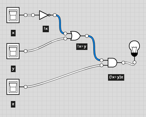
Expression to circuit diagram
In Logisim, draw this expression as a circuit: x'+y*z
Right

Wrong
Function tables
A function table is like a truth table; however, cells in the lower right quadrant can be logic expressions.
For example, here’s the truth table for a ⊕ b:
| a | b | a ⊕ b |
|---|---|---|
0 |
0 |
0 |
0 |
1 |
1 |
1 |
0 |
1 |
1 |
1 |
0 |
We can condense this down to this function table, by freeing variable b:
| a | a ⊕ b |
|---|---|
0 |
b |
1 |
b' |
Study this function table carefully in relation to the truth table above. We shrank down a truth table without losing information by noticing that a ⊕ b is the same as b if a is false, and a ⊕ b is the inverse of b if a is true.
September 8
Truth table → logic expression
September 10
Boolean algebra
Boolean algebra is very similar to plain algebra, but some laws are unique to Boolean algebra. For example, the distributive law, has a form unique to Boolean algebra.
Law |
Form |
Dual form |
Identity |
a * 1 = a |
a + 0 = a |
Commutative |
a * b = b * a |
a + b = b + a |
Associative |
(a * b) * c = a * (b * c) |
(a + b) + c = a + (b + c) |
Identity |
a * 0 = 0 |
a + 1 = 1 |
Distributive |
a * (b + c) = a * b + a * c |
a + (b * c) = (a + b) * (a + c) |
Idempotence |
a * a = a |
a + a = a |
Absorption |
a + a * b = a |
a * (a + b) = a |
Complement |
0' = 1 |
1' = 0 |
Complement |
a * a' = 0 |
a + a' = 1 |
Involution |
a'' = a |
a'' = a |
DeMorgan’s |
(a + b)' = a' * b' |
(a * b)' = a' + b' |
Dual forms
All laws of Boolean algebra come in two forms, the law and its dual form. The dual form of any valid equation in Boolean algebra is also true.
To find the dual form of a logic expression:
-
Evaluate the original expression and put parentheses around all subexpressions
-
Swap 1 with 0 (and vice versa)
-
Swap AND with OR (and vice versa)
-
Leave complements (NOT) alone
Notice how the steps above convert the form of a law to its dual form?
Example: Find the dual form of Z'+X*Y
This is Z'*(X+Y).
Challenge: Find the dual form of (a + b)' + c * a' + 1
Simplification
Apply the laws of Boolean algebra to an expression or equation to simplify/prove it. This is the sort of thing that’s easier said than done, and practice will help.
Hint: Work slowly and methodically: picture yourself working your way through a maze. Starting with the original expression, apply one law at a time until you arrive at the answer. At each step, you may choose many possible paths based on the laws you apply.
Example: Show X*Y'Z + X*Y*Z' + X*Y*Z = X(Y+Z)
X*Y'Z + X*Y*Z' + X*Y*Z = X(Y+Z) |
Original expression |
X*(Y'Z + Y*Z' + Y*Z) = X(Y+Z) |
Distributive law |
X*(Z*(Y' + Y) + Y*Z') = X*(Y+Z) |
Distributive law |
X*(Z*(1) + Y*Z') = X*(Y+Z) |
Complements |
X*(Z + Y*Z') = X*(Y+Z) |
Identity |
X*(Z + Z*Y + Y*Z') = X*(Y+Z) |
Absorption |
X*(Z + Y*(Z + Z')) = X*(Y+Z) |
Distributive law |
X*(Z + Y*(1)) = X*(Y+Z) |
Complements |
X*(Z + Y) = X*(Y+Z) |
Identity |
X*(Y + Z) = X*(Y+Z) |
Commutative law |
Challenge: Show (a * b)' * (a' + b) * (b' + b) = a'
Gray codes
A Gray code (also known as a reflected binary code) is a way of encoding binary numbers so that every increment changes only a single bit.
When we count in binary, we repeat 01 over and over again in the least significant place value. When we count in gray codes, we repeat 0110 over and over again in the rightmost bit.
Binary |
Decimal |
Gray code |
0000 |
0 |
0000 |
0001 |
1 |
0001 |
0010 |
0 |
0011 |
0011 |
1 |
0010 |
0100 |
0 |
0110 |
0101 |
1 |
0111 |
0110 |
0 |
0101 |
0111 |
1 |
0100 |
1000 |
0 |
1100 |
1001 |
1 |
1101 |
1010 |
0 |
1111 |
1011 |
1 |
1110 |
1100 |
0 |
1010 |
1101 |
1 |
1011 |
1110 |
0 |
1001 |
1111 |
1 |
1000 |
Binary → Gray code
-
Shift the number to the right by one bit
-
Bitwise XOR the number and the original number
In C, this is: (num >> 1) ^ num
Example: What is the Gray code for 0b10110?
10110 num
01011 num >> 1
11101 bitwise XOR (Gray code)
What’s the point?
Karnaugh maps (K-Maps)
Karnaugh maps:
-
are an alternate way of representing truth tables and function tables
-
layout a single output function and use the horizontal and vertical axes of a table for the values of the inputs
-
use Gray codes to ensure that related values go together spatially in the table
-
can help you find simple logic expressions
September 11
Lab 1. Due: By next Friday at the latest.
Save your work in a file called lab1.txt in your repo.
cd ~/COMP2270-2015
touch lab1.txt
|
Note
|
Use a proper text editor, such as this. |
Number representation
-
Convert 1590 to binary.
-
Convert 0b101110110 to decimal.
-
Convert 0b1100 0000 0001 1010 0001 0101 1011 1010 1101 to hexadecimal.
-
Convert 0b100 001 101 101 to octal.
-
Convert 0o31337 to binary.
-
Convert 0xBADF00D to binary and then to octal.
-
Convert 0o6157 to binary and then to decimal.
-
Convert 497 to binary. Then, use two’s complement to convert 497 to -497 in binary.
-
Convert 900.79 to binary up to the 1/16ths spot.
-
Count from 0 through 10 in ternary (base 3). Note: the algorithm for counting is similar regardless of the number base. Show the place values.
Circuit design
-
Let A and B be two 2-bit binary numbers (i.e., A1 A0 and B1 B0). Write out a truth table for A less than or equal to B. For example, 0b10 is less than or equal to 0b11, so the output for that row should be true.
-
Write out the equivalent logic expression for the previous answer.
-
Write out the truth table for the minority circuit (it’s true when the minority of X, Y, and Z are true).
-
Write out the equivalent logic expression for the previous answer.
Boolean algebra
Use the laws of Boolean algebra.
-
Show c + (b * c)' = 1
-
Show (a + c) * (a * d + a * d') + a * c + c = a + c
-
Simplify a' * (a + b) + (b + a * a) * (a + b')
-
Show (a' * b') + (a' * b) + (a * b') = (a * b)'
Dual form
Find the dual form.
-
(a + b)' + c * a' + 1
-
1 + 1 * 0'
How to submit work
Stage → Commit → Push
cd ~/COMP2270-2015
touch lab1.txt
git add lab1.txt
git commit -m "Added lab 1 solution."
git push origin master
September 15
Function tables
Function tables are a way to compact down a truth table by removing variable(s) from the input columns and placing it into the output function. Function tables are so called because the outputs are no longer merely just 0 or 1, but also any function of input variables.
Example
Here’s the truth table for a ⊕ b:
| a | b | a ⊕ b |
|---|---|---|
0 |
0 |
0 |
0 |
1 |
1 |
1 |
0 |
1 |
1 |
1 |
0 |
We can condense this down to this function table, by freeing variable b:
| a | a ⊕ b |
|---|---|
0 |
b |
1 |
b' |
Notice how when a is false, the output function is the same as b. When a is true, the output function is the inverse of b.
Multiplexers
Multiplexers (MUX) are circuits that redirect one of several inputs to a single output based on the value of the selector. That is, the output corresponds to the selected input.
In this respect, multiplexers are equivalent to switch/case statements.
boolean Four1MUX(byte selector, boolean input0, boolean input1, boolean input2, boolean input3) {
    switch(selector) {
        case 0: return input0;
        case 1: return input1;
        case 2: return input2;
        case 3: return input3;
    }
    return false;
}
The function table for a 4-1 MUX (4 input, 1 output multiplexer) is as follows:
| S1 | S0 | Output |
|---|---|---|
0 |
0 |
Input0 |
0 |
1 |
Input1 |
1 |
0 |
Input2 |
1 |
1 |
Input3 |
Select bits S1 and S0 represent the most and least significant bits of S (respectively) in binary.
Truth/function table to multiplexer
To implement a combination logic function with a multiplexer, the number of rows (excluding the header) in the truth/function table must equal the number of inputs to the multiplexer. If your truth table has more rows than the multiplexer has inputs, write out a function table with the same number of inputs as the multiplexer equivalent to the truth table.
-
Align the outputs of your table to the inputs of the multiplexer.
-
The select bits will correspond to the input variables.
-
Ta-da!
September 17
Combinational vs. Sequential logic
At this point, everything we’ve talked about has concerned combinational logic. In combinational logic, outputs are functions of inputs. In other words, combinational logic has no memory.
Today, we’ll talk about sequential logic. In sequential logic, outputs are functions of inputs and prior outputs. Put another way, sequential logic is combinational logic + memory.
Latches
Latches are a single bit memory device. We can construct a latch using two NAND gates or two NOR gates. We have two inputs, S' and R', and an output Q. These are fed as input to the separate gates, leaving each gate with an empty pin for another input. The other input to each gate is the output of the other gate. Thus, the gates are cross-connected to each other, so the output is literally a function of inputs and prior outputs.
In a latch, we can describe the behavior using a characteristic table, similar to a truth table. In a characteristic table, we describe the behavior of the circuit.
(SR)' NAND latch characteristic table
S' |
R' |
Q |
0 |
0 |
Restricted state (here be dragons) |
0 |
1 |
Q=1 (Assign Q to 1) |
1 |
0 |
Q=0 (Assign Q to 0) |
1 |
1 |
No change |
Try it out for yourself.
Latches are so called because they are level-triggered. Level-triggered means that the level (hi or lo voltage) of the input is what causes the value of Q (the memory) to change.
Flip-flops
Flip-flops, like latches, are a single bit memory device. Unlike latches, flip-flops are edge-triggered. Edge-triggered means that the transition from one input to another is what causes the value of the memory to change. There are two kinds of edge: rising edge (positive edge) and falling edge (negative edge), corresponding to the transition from low to hi and hi to lo, respectively.
Flip-flops are made from latches, but with extra circuitry to make it edge-triggered. The circuitry itself takes advantage of solid-state physics to achieve the desired effect. Just as the speed of sound varies based on the medium (e.g., air, water), or the speed of light varies based on the medium (e.g., vacuum, fiber-optics, air), the speed at which electrons flow through a circuit varies based on the medium. Electrons flow at nearly the speed of light through good conductors such as copper, but flow slightly slower through semiconductors such as silicon (known as a gate propagation delay ).
The expression x'+x is always equal to 1, but the circuit implementing this isn’t always equal to 1, because of gate propagation delays.
Registers
A register is a multiple-bit memory device. Registers are multiple flip-flops chained together to store things like integers, characters, and such. When you declare a variable, like int i = 0, the compiler allocates i to a register and sets the value of that register. Most CPUs have at least two registers in them.
September 18
Lab 2: Combinational circuit design
Deadline: By the next lab.
Implement a full adder (a + b + cin) using two 4-1 multiplexers (one multiplexer for carry out, one multiplexer for sum, using the same input variables).
|
Note
|
To test your work, use an adder (Arithmetic → Adder), using a single data bit. |
Carry-in |
A |
B |
Carry-out |
Sum (A+B) |
0 |
0 |
0 |
0 |
0 |
0 |
0 |
1 |
0 |
1 |
0 |
1 |
0 |
0 |
1 |
0 |
1 |
1 |
1 |
0 |
1 |
0 |
0 |
0 |
1 |
1 |
0 |
1 |
1 |
0 |
1 |
1 |
0 |
1 |
0 |
1 |
1 |
1 |
1 |
1 |
Sequential design: Even/Odd number of zeroes and ones

-
Answer these questions about the state machine above.
-
How many bits for state will you need?
-
How many input bits will you need?
-
-
Then, map states to bits, and map inputs to bits.
-
Write out a state-transition table.
-
Finally, program a ROM to do said thing.
Vending machine

-
Answer these questions about the state machine above.
-
List all possible inputs. How many do we have?
-
List all possible states. How many do we have?
-
How many bits for state will you need?
-
How many input bits will you need?
-
-
Then, map states to bits, and map inputs to bits.
-
Write out a state-transition table. Since 25 cents is the final state, what happens if we get extra currency? Or, what happens if we get foreign currency? Feel free to transition to a "bogus" state (or states) for these purposes.
-
How many bits will we need for ROM address?
-
How many bits will we need for ROM data?
-
Finally, use a ROM to implement said thing.
When you are done, save your work and do the following:
cd ~/COMP2270-2015
git add lab2solution.*           # Stage your changes to the next commit
git commit -am "Lab 2 complete." # Record your changes locally
git push origin master           # Push your work
September 22
Continue Lab 2.
cd ~/COMP2270-2015
git pull upstream master
# If you see the word CONFLICT
git mergetool
start .    # On Windows
open .     # On Mac
xdg-open . # On Linux
September 24
Out sick.
September 25
Out sick
September 29
-
How to know you submitted work correctly
-
Lab 2 walkthrough
October 1
-
Lab 2 walkthrough (continued)
October 2
October 6
Midterm review
October 8
Midterm review? Again? Srsly?
October 9
Midterm
October 13
October 15
Hand back midterms
October 16
Lab 3: Assembly/Machine language programming
It’s like CS1 all over again!
Maximum
-
Write out source code for a function that computes the maximum of two numbers. (Yes, I know practically every language has a
max(a,b)function, I want you to write your own version).
int a = RAM[0x80]
int b = RAM[0x81]
int max = a;
if (b > a) {
    max = b;
}
-
Write out equivalent assembly code for source code. One stipulation: the two numbers should be loaded from RAM. Hint: the STOR instruction doesn’t work. Store the result into a register. To move data from Rs to Rd, ADD Rd, Rs, R0 (R0 is constant 0).
-
Write out equivalent machine code, and test it in Logisim, using the supplied CPU in
circuits/cpu-16bit.circ. -
Save the contents of RAM as lab3max.txt.
Sum
-
Write out source code for a function that computes the sum of an array of integers. (Yes, I know practically every language has a sum(array) function, I want you to write your own version). Write it with the assumption that the length is given separately from the array:
int sum(int length, int[] array); -
Write out equivalent assembly code for source code. One stipulation: the array should be loaded from RAM, and the size of the array should be read first. Hint: use the LOAD Ra instruction (opcode d in hex).
-
Write out equivalent machine code, and test it in Logisim, using the supplied CPU in
circuits/cpu-16bit.circ. -
Save the contents of RAM as lab3sum.txt.
When you are done, save your work and do the following:
git add lab3*                    # Stage your changes to the next commit
git commit -am "Lab 3 complete." # Record your changes locally
git push origin master           # Push your work
October 21
Welcome to the future
October 22
October 23
Lab 4.
Grab my changes
cd ~/COMP2270-2015
git checkout -- circuits/cpu-16bit.circ
git pull upstream master
git checkout --theirs circuits/cpu-16bit.circ
git add circuits/cpu-16bit.circ
git status
git commit -m "Fixed merge conflict."
Logic gates to ROM
Open circuits/cpu-16bit.circ in Logisim.
Replace the bus control’s contents with a ROM, but leave the multiplexer alone, as show below:
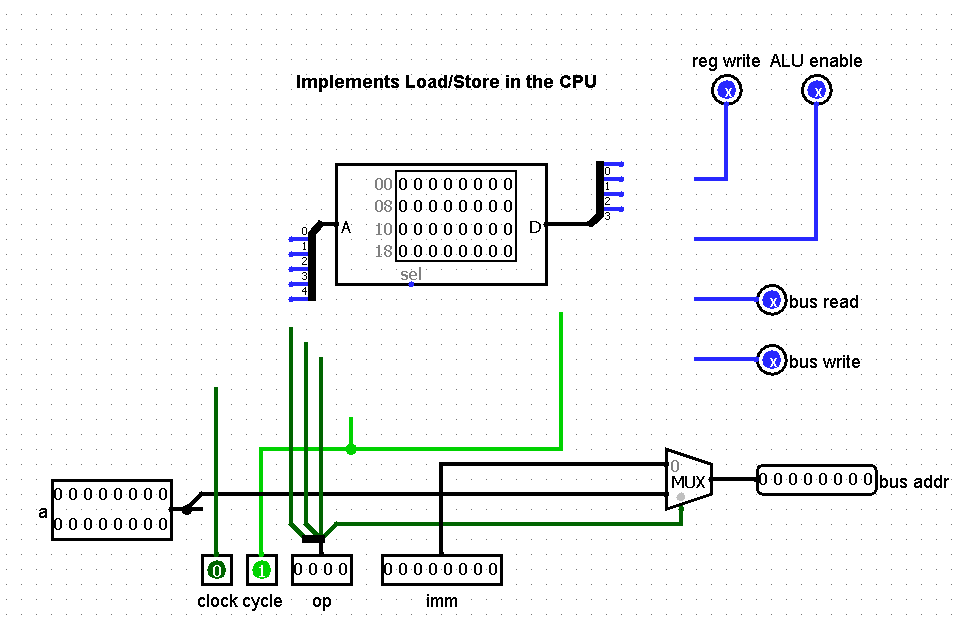
The ROM should have 5 input (address) bits (corresponding to clock, cycle and op’s 3 MSBs), and 4 output (data) bits (corresponding to reg write, ALU enable, bus read, bus write). We don’t need the least significant bit of the opcode, because it does not influence the output in any way.
Hint: poke on inputs to see what the corresponding output is, and note that in the table below (also available in labs/bus-control-rom.csv).
Then, take that table, and program (and connect) the ROM accordingly.
|
Note
|
There’s no state involved, it’s purely combinational. |
|
Important
|
Test your CPU to ensure that your code from lab 3 is still functional. If not, you goofed up. |
| ROM address | Clock | Cycle | Op3 | Op2 | Op1 | Reg write | ALU enable | Bus read | Bus write | |
|---|---|---|---|---|---|---|---|---|---|---|
0 |
0 |
0 |
0 |
0 |
0 |
|||||
1 |
0 |
0 |
0 |
0 |
1 |
|||||
2 |
0 |
0 |
0 |
1 |
0 |
|||||
3 |
0 |
0 |
0 |
1 |
1 |
|||||
4 |
0 |
0 |
1 |
0 |
0 |
|||||
5 |
0 |
0 |
1 |
0 |
1 |
|||||
6 |
0 |
0 |
1 |
1 |
0 |
|||||
7 |
0 |
0 |
1 |
1 |
1 |
|||||
8 |
0 |
1 |
0 |
0 |
0 |
|||||
9 |
0 |
1 |
0 |
0 |
1 |
|||||
10 |
0 |
1 |
0 |
1 |
0 |
|||||
11 |
0 |
1 |
0 |
1 |
1 |
|||||
12 |
0 |
1 |
1 |
0 |
0 |
|||||
13 |
0 |
1 |
1 |
0 |
1 |
|||||
14 |
0 |
1 |
1 |
1 |
0 |
|||||
15 |
0 |
1 |
1 |
1 |
1 |
|||||
16 |
1 |
0 |
0 |
0 |
0 |
|||||
17 |
1 |
0 |
0 |
0 |
1 |
|||||
18 |
1 |
0 |
0 |
1 |
0 |
|||||
19 |
1 |
0 |
0 |
1 |
1 |
|||||
20 |
1 |
0 |
1 |
0 |
0 |
|||||
21 |
1 |
0 |
1 |
0 |
1 |
|||||
22 |
1 |
0 |
1 |
1 |
0 |
|||||
23 |
1 |
0 |
1 |
1 |
1 |
|||||
24 |
1 |
1 |
0 |
0 |
0 |
|||||
25 |
1 |
1 |
0 |
0 |
1 |
|||||
26 |
1 |
1 |
0 |
1 |
0 |
|||||
27 |
1 |
1 |
0 |
1 |
1 |
|||||
28 |
1 |
1 |
1 |
0 |
0 |
|||||
29 |
1 |
1 |
1 |
0 |
1 |
|||||
30 |
1 |
1 |
1 |
1 |
0 |
|||||
31 |
1 |
1 |
1 |
1 |
1 |
Fix the store instruction
Make the store instruction work. I’ll show how to fix it. Hint: the RAM could be changed a bit to fix it without much grief.
Submission
Assuming that you save your work in circuits/cpu-16bit.circ, just do:
cd ~/COMP2270-2015
git commit -am "Lab 4 done."
git push origin master
If you saved your work somewhere else, be sure to stage (git add the file).