New V3 board with audio fix has been submitted. Check the kicad folder for gerbers. It requires few new components that you can read on the board. Pretty simple: 10uf capacitor and an optional cinch connector. I will not be updating the BOM lists. WIP project. For a 9958 socket, turn off GromClk (Jumper 3). Leave CpuClk on (Jumper4).
The V9958 drop-in socket (SDIP-64) has been submitted. Check the kicad folder. Code has been improved for Omega MSX compatibility. SDIP pin header are hard to find. Check AliExpress for "1.778mm Pitch Single Row Male Round Pin Header". Not including links they aren't persistent. You need a V3 main board as well for the Tang20K.
Note My Omega MSX has the RAM expansion module and I found out it has incompatiblity with the Tang (seems to be too noisy). If you get issues with IDE controllers, try removing some RAM chips from higher banks. I left my Omega with only 2MB. It's not a PSU problem but rather a routing issue that plagues the Omega for some time.
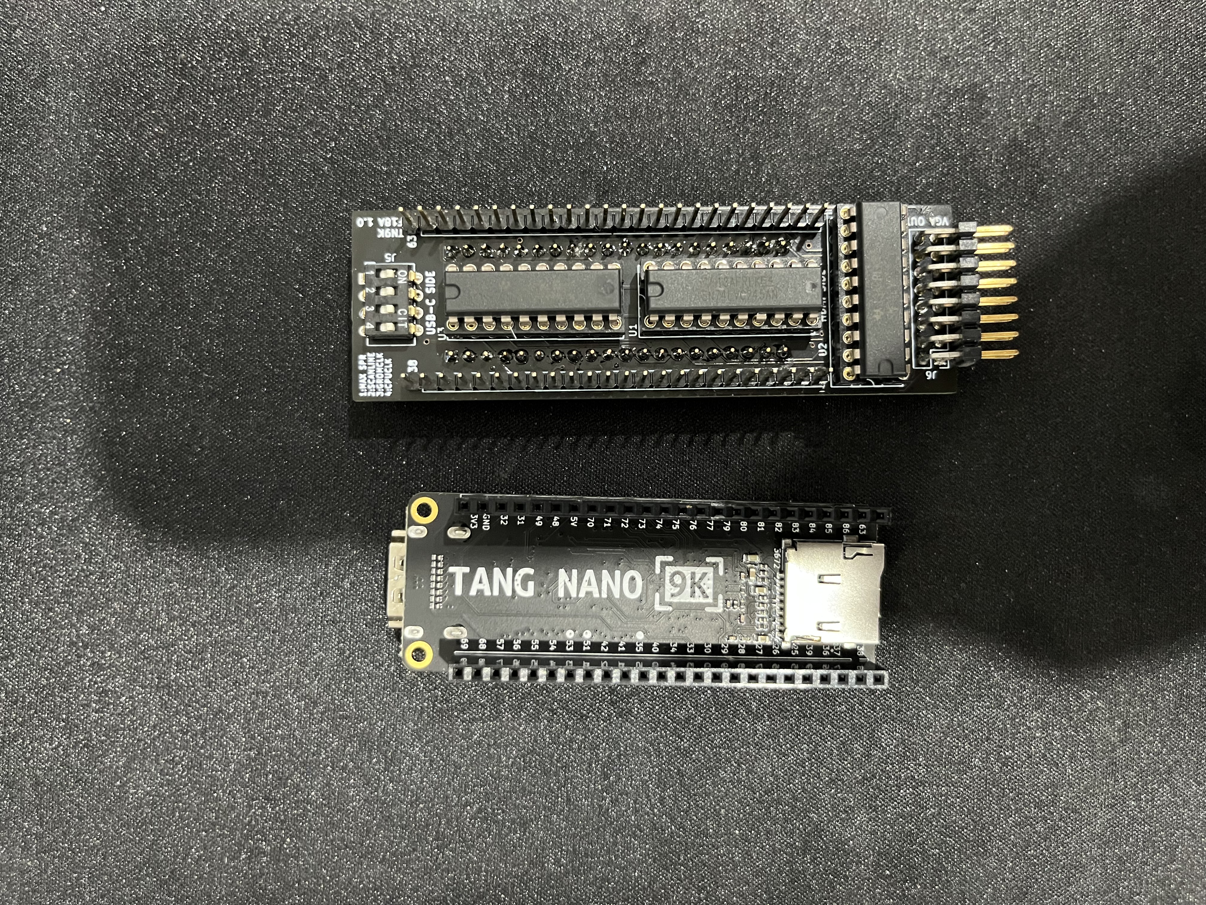
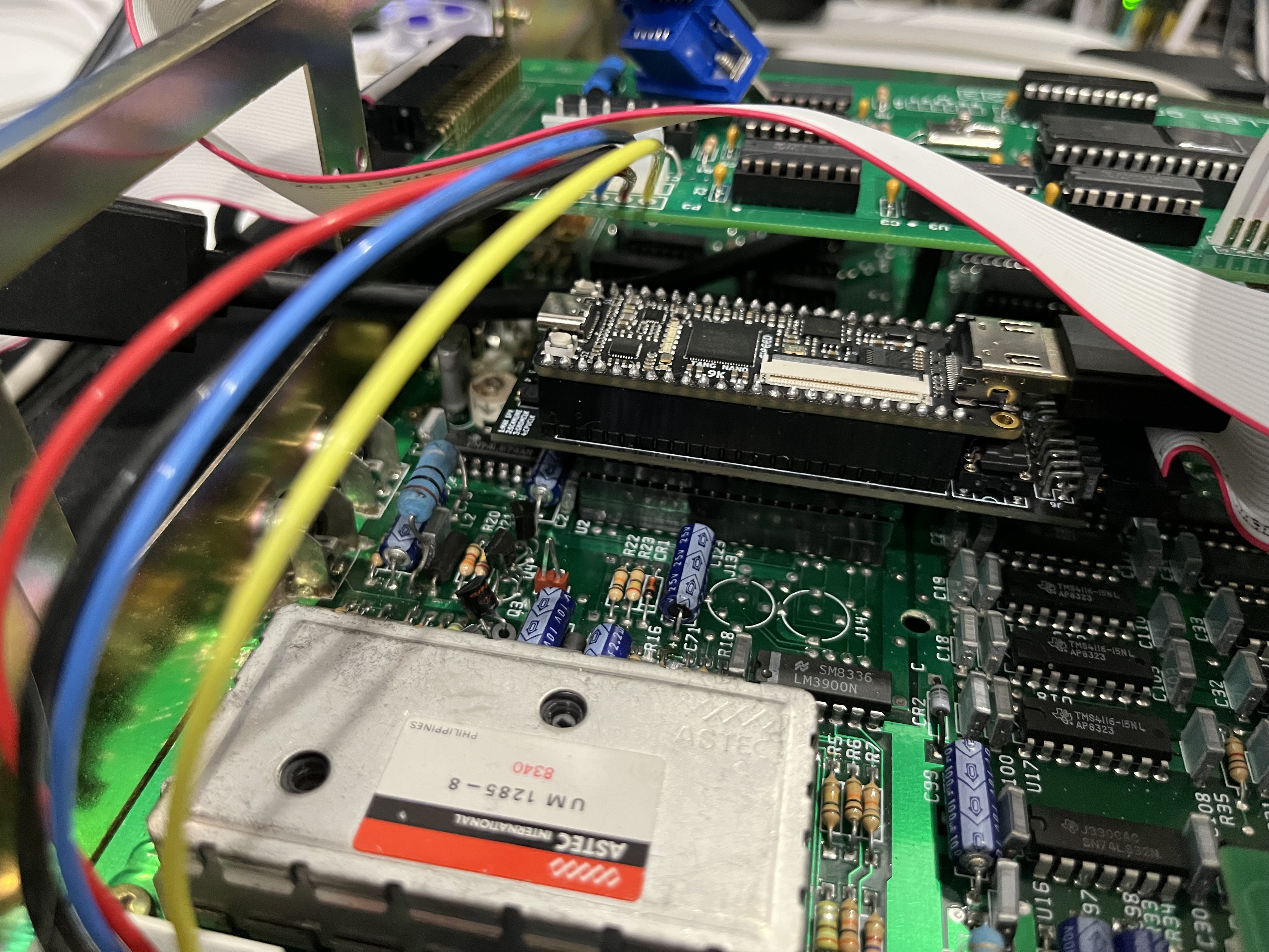
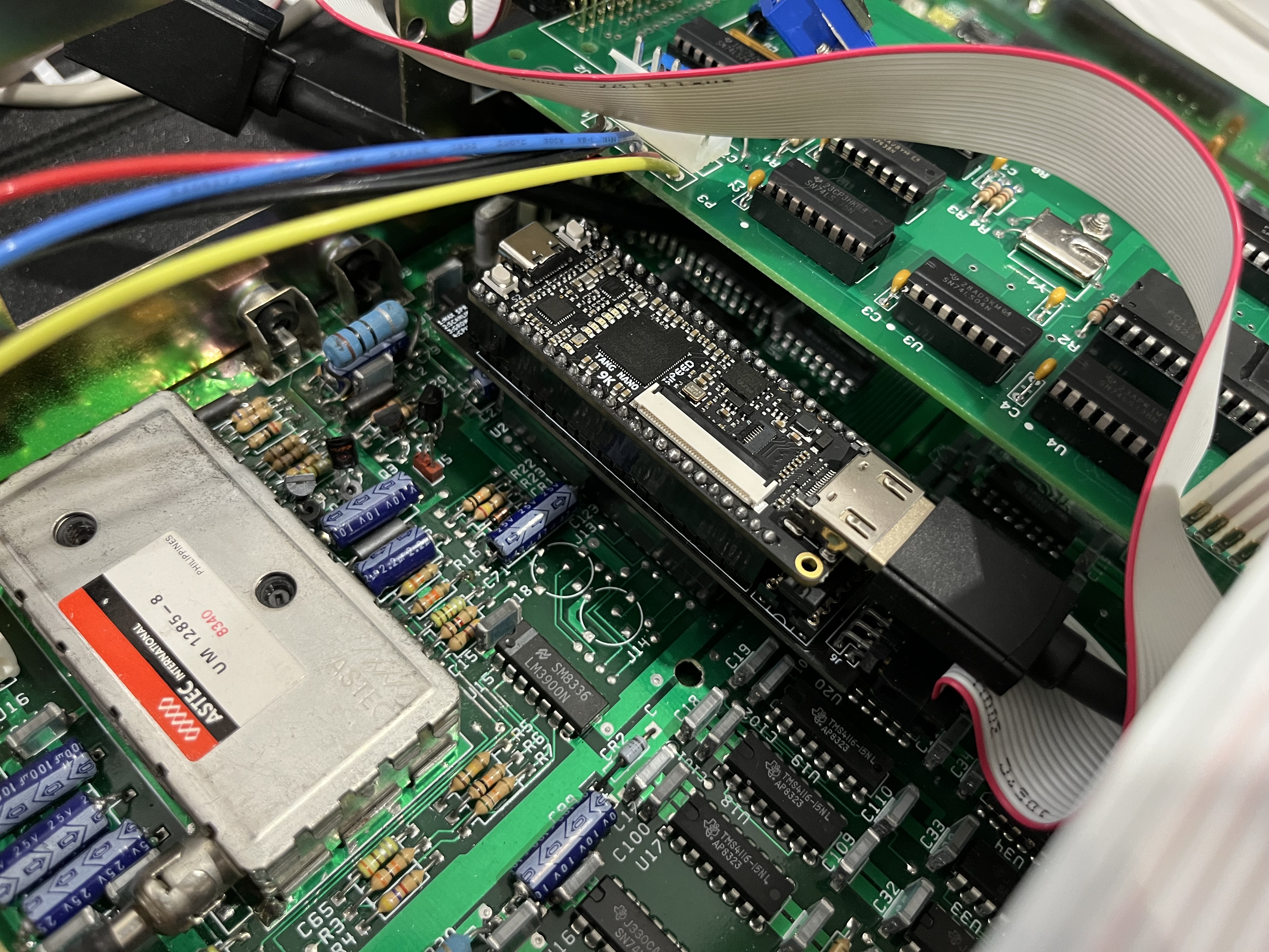
This project recreates the TMS9118A (and its TMS9928A/TMS9929A variants) in FPGA using the over the counter Sipeed's Tang Nano 9K board plus a designed set of boards to be stacked on top where the TMS9118 was located.
TN VDP v1 uses Matthew Haggerty's F18A core, which is completely compatible with the original Texas Instruments VDP, but adds additional video modes, sprites and color capabilities.
The bitstream file is here
The new version supports audio over HDMI. There is no more VGA output. You'll need to pull the pre-amplified audio from somewhere in the computer and connect the AUDIO pin on the tn-vdp socket. MODE1 is not used for TMS9918 cores.
This requires the v2 board sets as well the v2 bitstream (socket board + mainboard). See below gerber files.
There are 2 bitstreams for v2:
There is a new core for the v2 boards implemented from ESE-MSX3. The bitstream can be used on the same v2 board sets for the TMS9918:
But for the V9958 you need to pull the A1 address line from somewhere in the computer and connect to pin MODE1 on the socket to use the full capabilites of the V9958.
The v3 of the fpga code and mainboard is for use on a Tang Nano 20K only. There are no other versions for Tang Nano 20K other than V9958 128K. If you need a 9918 use the Tang Nano 9K instead. The socket for the TMS9118 is the same from v2. A socket for a V9958 replacement is in the works.
See instructions below for programming it.
Note The gromclk signal has been retired from V9958 128K (no MSX ever uses it). So instead turning this jumper on puts the VDP in no-wait mode, full speed 27Mhz. Turning off it makes the VDP at normal speed (for VDP commands).
Bootable 80 colums for NABU PC CP/M 3 images can be downloaded here (flux and HxC2001):
The gerber files can be located inside each KiCad project:
Compact board using SMD components See the separate README for BOM ipand additional information.
The VGA module is optional, only if you want VGA output.
Socket v2 (same TMS9918 socket as v2)
Follow this link to install the Gowin's IDE:
Note: The code can be built and programmed using the latest Education Version 1.9.8.11 - The Education EDA does not require a license. DO NOT USE THE BETA EDA/PROGRAMMER.
The FPGA series is GW1NR and the Device is GW1NR-9C. Use Embedded Flash Mode for permanent programming. Make sure the bitstream is set to Load Rate of 25Mhz (or higher) in the Project -> Configuration -> BitStream: Loading Rate (MHZ). The maximum for this device is 25 Mhz.
Gowin Programmer Together Gowin IDE you find the programmer or you can install the programmer stand alone. Check the Gowin IDE instructions
openFPGALoader Alternatively you can use the openFPGALoader but it requires changing the FTDI drivers through zadig. Follow the official page for instructions
The openFPGALoader tool can be used to program the FPGA from the command line.
sudo openFPGALoader -b tangnano9k tn_vdp.fs
The board has a standalone boot screen when you connect it to the USB-C and HDMI only. This will tell the FPGA has been programmed with success.
The v3 Tang Nano 20K has no standalone boot screen.
The Tang Nano 9K board can be purchased on AliExpress or ebay.
The boards gerber files are inside each kicad project gerber folders.
The BOM for the NABU and FAT v1 variants can be found here DigiKey BOM
Or transcribed here
Qty | Part Number                | Description
----+----------------------------+----------------------------------
1x  | 123-A-HDF15A-KG-TAXB-ND    | CONN D-SUB HD RCPT 15P R/A SLDR
3x  | 123-AR20-HZL-TT-ND         | CONN IC DIP SOCKET 20POS TIN
2x  | S7022-ND                   | CONN HDR 24POS 0.1 TIN PCB
1x  | 449-KT04RTH-ND             | SWITCH SLIDE DIP 4POS 25MA 24V
3x  | 296-8503-5-ND              | IC TXRX NON-INVERT 3.6V 20DIP
3x  | 1109PHCT-ND CAP            | CER 0.1UF 50V X7R AXIAL
2x  | 2057-PH2RA-16-UA-ND        | CONN HEADER R/A 16POS 2.54MM
2x  | A835AR-ND                  | CONN HDR DIP POST 20POS GOLD
1x  | ED3048-5-ND                | CONN IC DIP SOCKET 40POS TIN
1x  | 2057-ICM-640-1-GT-HT-ND    | MACHINE PIN SOCKET, IC, DIP, 40P
1x  | 1528-5294-ND               | GPIO RIBBON CABLE 2X10 IDC CABLE
3x  | CF14JT2K20CT-ND            | RES 2.2K OHM 5% 1/4W AXIAL
2x  | CF14JT47R0CT-ND            | RES 47 OHM 5% 1/4W AXIAL
3x  | CF14JT4K70CT-ND            | RES 4.7K OHM 5% 1/4W AXIAL
3x  | CF14JT1K00CT-ND            | RES 1K OHM 5% 1/4W AXIAL
3x  | F14JT470RCT-ND             | RES 470 OHM 5% 1/4W AXIAL
1x  | 497-4547-1-ND              | DIODE SCHOTTKY 20V 1A DO41
Notes:
- CONN HDR DIP POST 20POS GOLD: It is expensive on DigiKey but it can be sourced elsewhere cheaper, even Amazon.
- GPIO RIBBON CABLE 2X10 IDC CABLE : It was supposed to be 2x8 but is out of stock. The 2x10 just works. Or build your own.
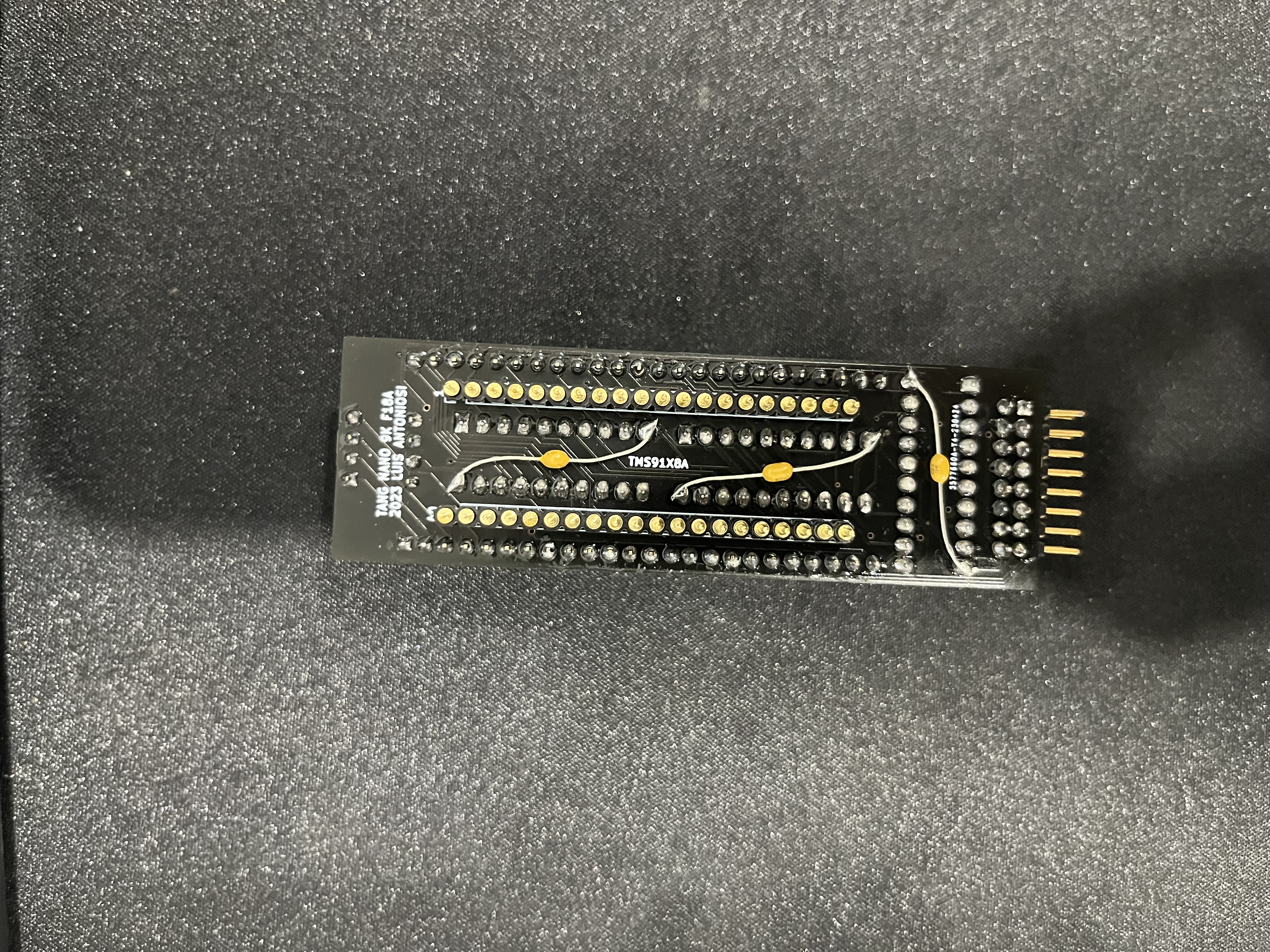
- The capacitors need to be soldered manually on the bottom of each IC's. There are no pads for them to reduce the size of the board. See back.jpg photo for reference under images folder.
- There are 2 DIP 40 sockets in this list: one machined other normal. The machined socket you will use to connect the board on top, thus protecting the pins. The machined pins for the board will connect easily to a machined socket. Then you stack this machined socked over the normal one (notice little force is necessary), and then finally you stack them at the NABU PC's TMS9118 socket. This will protect both the NABU and the tn_vdp pins.
Qty | Part Number                | Description
----+----------------------------+----------------------------------
3x  | 123-AR20-HZL-TT-ND         | CONN IC DIP SOCKET 20POS TIN
1x  | 2057-ICM-308-1-GT-HT-ND    | MACHINE PIN SOCKET, IC, DIP, 8P
3x  | 296-8503-5-ND              | IC TXRX NON-INVERT 3.6V 20DIP
4x  | BC1084CT-ND                | CAP CER 0.1UF 50V X7R RADIAL
1x  | 1528-5294-ND               | GPIO RIBBON CABLE 2X10 IDC CABLE
1x  | 497-4547-1-ND              | DIODE SCHOTTKY 20V 1A DO41
1x  | MCP3202-CI/P-ND            | IC ADC 12BIT SAR 8DIP
2x  | S7022-ND                   | CONN HDR 24POS 0.1 TIN PCB
2x  | A835AR-ND                  | CONN HDR DIP POST 20POS GOLD
4x  | 732-5301-ND                | CONN HEADER VERT 20POS 2.54MM
1x  | 10129379-920001BLF-ND      | CONN HEADER R/A 20POS 2.54MM
4x  | S9000-ND                   | CONN JUMPER SHORTING TIN
Notes:
I find these header pins 2.54mm too expensive on DigiKey. I'd advise you to procure them on AliExpress, longer wait time but way cheaper.
The V3 BOM is almost identically to V2 except that I added a trimmer for the audio and I returned with the DIP switch 4 pos:
Qty | Part Number                | Description
----+----------------------------+----------------------------------
1x  | 3339P-1-103LF              | TRIMMER 10K OHM 0.5W PC PIN TOP
1x  | 449-KT04RTH-ND             | SWITCH SLIDE DIP 4POS 25MA 24V
These are the jumper. Closed means ON:
USR1 : SPR MAX - Turn it on for 32 sprites per line (9958 this puts 8 sprites for mode 0)
USR2 : SCANLIN - Turn it on for scanlines
USR3 : GROMCLK - Turn it on to have GROM CLOCK enabled, Disabling it puts CPUCLK on pin 37 (9128/29)
USR4 : CPUCLK  - Turn if on to have CPU CLOCK on pin 38 (9929/29 and 9128/29)
You shouldn't have problem assembling it as all components are labeled. Just remember the 2 pin strips for the TMS9118 slot goes under the board as well the 3 caps. Everything else it on the top side. I personally prefer soldering the female header on the FPGA board. Mind the orientation of the DIP switch as the image below.
1) solder the 3 DIP-20 sockets on top side
2) for each socket, solder one axial caps under the board connecting pins GND and VCC the back image below
3) solder the mini-switch on top side, mind hte numbering according to the text
4) solder the two male machine strips under the board (20 pins each strip)
5) solder the male pins that came with the Tang Nano 9K board on the top side of the board (24 pins each)
6) solder the 8x2 right angle header (optional for VGA)
6) solder the 2 female headers under the Tang Nano 9K board
7) install the 3 74VLC256 chips. Mind the half-moon orientation
7) plug the Tang Nano 9K on the male pins, mind the HDMI and UBS-C orientation as printed on the board
8) configure the dip-switches
USR1 - 32 sprite per line (TMS9918), 8 sprites per line (V9958)
USR2 - scanlines
USR3 - pin 37: gromclk (on), cpuclk (off)
USR4 - pin 38: cpuclk (on), NC (off)

TMS9918A: (NABU-PC, CX5M)
USR3 - on
USR4 - on

TMS9928/29A
USR3 - on
USR4 - off

TMS9918
USR3 - on
USR4 - on

TMS9128/29
USR3 - off
USR4 - off
The Tang Nano 20K version is a bit more convoluted to install. We need to reconfigure the PLL nets.
First using the programmer flash this LITEX on the board:
Disconnect and re-connect to your PC.
Go to device manager and change the properties for the USB Serial Port (COMxx) for your Tang Nano 20K (disconnect/reconnect the board and see wich one disappear to identify it). Change the Port Settings: Bits per second to 115200 and Apply.
Now you need a terminal application like Tera Term to connect to serial port.
Pressione Control-X Control-C and ENTER
You should see the LITE terminal, type:
pll_clk O0=50M
pll_clk O1=125M
pll_clk -s
After that you can just flash the v3 core from here:
Now the board is ready to use.
You need to solder the capacitors under each IC's. I made this way to reduce the size of the board.
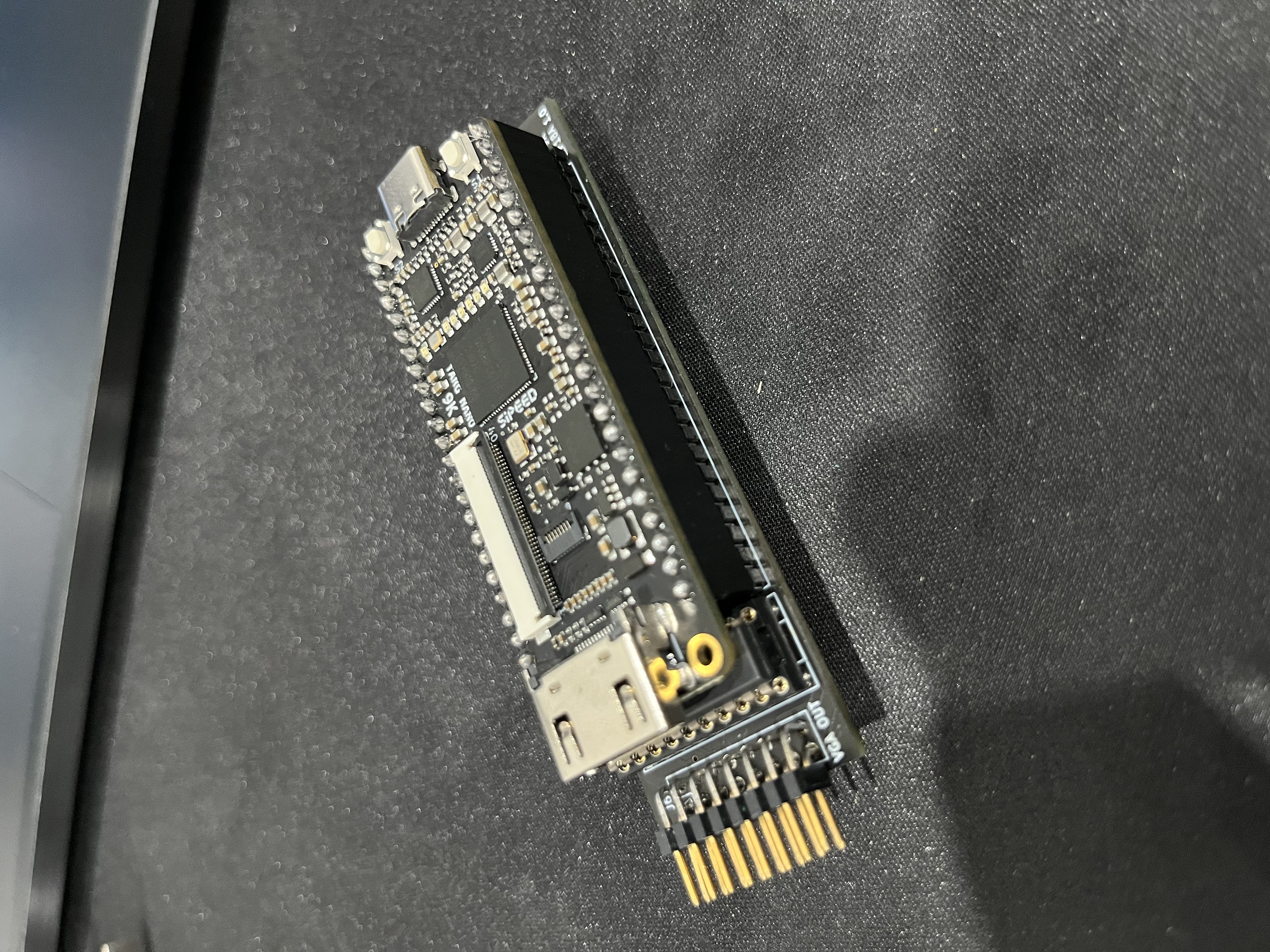
And the final board stacked up. To avoid plugging the board inverted there are two labels on it: USB-C SIDE and HDMI SIDE. The orientation of the board towards the TMS9118 slot is the USB-C up (pin 1 of TMS9118). The TMS9118 pin number 1 and 40 are printed under it.

