Replica of a 386SX Mainboard
- V0.1 Initial revision 2022 made with Sprint-Layout
- V0.2 Silkscreen updated, component positions and mounting holes modified
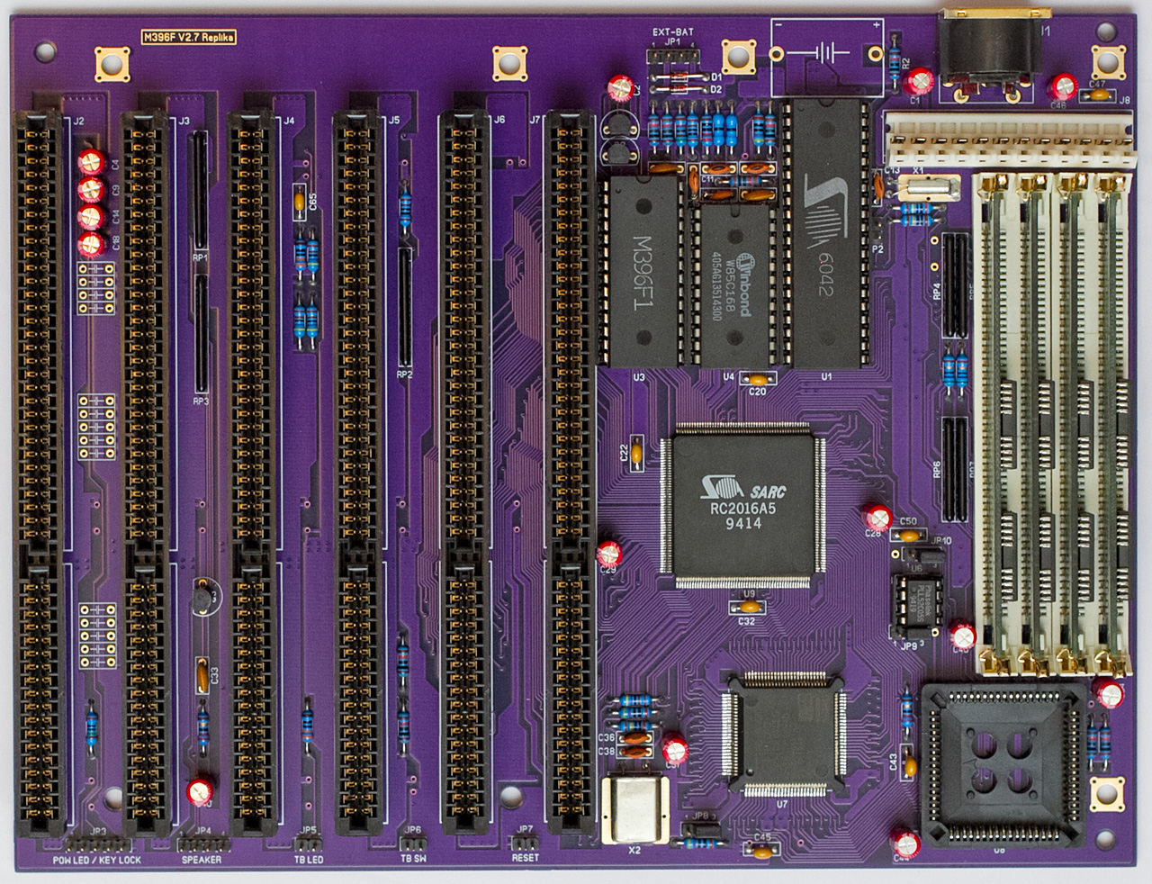
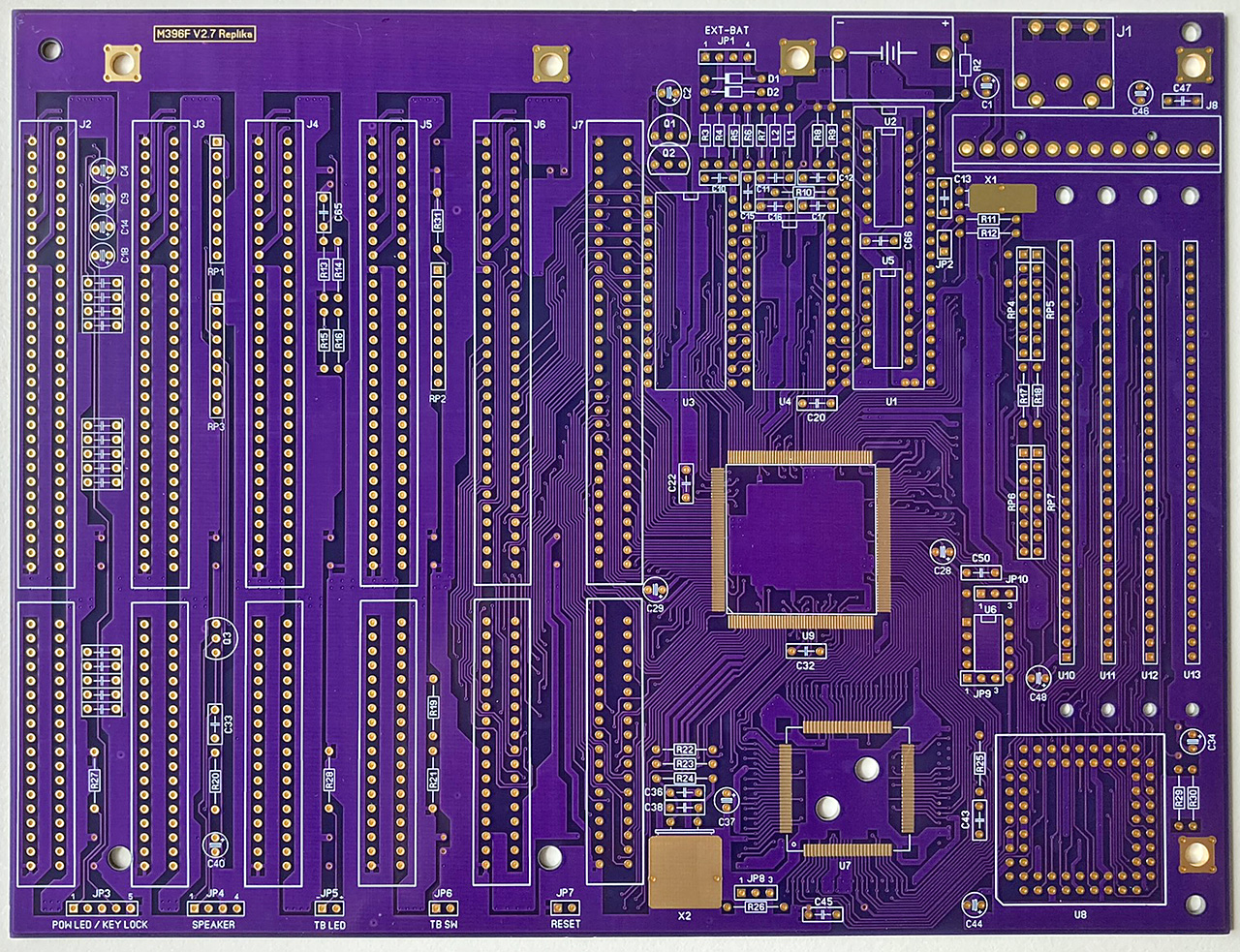
This replica of a 386SX motherboard is based on the SARC RC2016A chipset. Supported are 386SX or CX486SLC 25/33/40 MHz CPUs. A socket for the optional 80387SX coprocessor is available. The RAM reaches from 512kb to 16MB. I recommend faster 60ns RAM. The manual, jumper settings and useful downloads can be found here https://theretroweb.com/motherboards/s/pcchips-m396f-ver.2.6#downloads
| Quantity | Description | PCB/Schematic's Reference |
|---|---|---|
| 4 | CAP CER 30 pF RM 5,0 | C11, C13, C36, C38 |
| 3 | CAP CER 47 pF RM 5,0 | C12, C15, C66 |
| 1 | CAP CER 220 pF | CXX (Backside see notice) |
| 1 | CAP CER 4,7 nF RM 5,0 | C16 |
| 1 | CAP CER 100 pF nF RM 5,0 | C65 |
| 10 | CAP CER 100 nF RM 5,0 | C10, C17, C20, C22, C32, C33, C43, C45, C47, C50 |
| 14 | CAP ELKO 10 uF 25V RM 2,5 | C1, C2, C4, C9, C14, C18, C28, C29, C34, C37, C40, C44, C46, C48 |
| 2 | DIODE 1N4148 | D1, D2 |
| 6 | 16 Bit ISA Socket | J2, J3, J4, J5, J6, J7 |
| 1 | AT Power connector | J8 |
| 1 | Battery | BAT |
| 1 | CON 4 PIN | JP1 external Battery |
| 1 | CON 2 PIN | JP2 Display type |
| 1 | CON 5 PIN | JP3 Power LED / Key lock |
| 1 | CON 4 PIN | JP4 Speaker |
| 1 | CON 2 PIN | JP5 Turbo LED |
| 1 | CON 2 PIN | JP6 Turbo switch |
| 1 | CON 2 PIN | JP7 Reset switch |
| 3 | CON 3 PIN | JP8, JP9, JP10 CPU clock select |
| 1 | 3906 | Q1 |
| 2 | 3904 | Q2, Q3 |
| 2 | RES 0 Ohm 5% 1/4W | L1, L2 |
| 2 | RES 22 Ohm 5% 1/4W | R20, R25 |
| 2 | RES 56 Ohm 5% 1/4W | R17, R18 |
| 1 | RES 150 Ohm 5% 1/4W | R27 |
| 1 | RES 220 Ohm 5% 1W | R7 |
| 2 | RES 330 Ohm 5% 1/4W | R13, R28 |
| 3 | RES 470 Ohm 5% 1W | R8, R23, R26 |
| 2 | RES 1 k Ohm 5% 1/4W | R6, R31 |
| 4 | RES 4,7 k Ohm 5% 1/4W | R14, R15, R16, R22 |
| 9 | RES 10 k Ohm 5% 1/4W | R2, R3, R4, R9, R10, R19, R21, R29, R30 |
| 1 | RES 51 k Ohm 5% 1/4W | R5 |
| 2 | RES 1 M Ohm 5% 1/4W | R12, R24 |
| 1 | RES 2 M Ohm 5% 1/4W | R11 |
| 2 | RES Network 4,7 k Ohm bussed | RP1, RP2 |
| 1 | RES Network 330 Ohm bussed | RP3 |
| 3 | RES Network 10 Ohm parallel | RP4, RP5, RP6 |
| 1 | RES Network 100 Ohm parallel | RP7 |
| 1 | IC SARC 6042 o. VIA VT82C42 | U1 |
| 1 | IC 74HC05AP | U2 |
| 1 | IC BIOS | U3 |
| 1 | IC W85C168 | U4 |
| 1 | IC TC4069UBP | U5 |
| 1 | IC PLL52C05S o. TK9107-2 | U6 |
| 1 | IC CPU | U7 |
| 1 | IC Coprocessor | U8 |
| 1 | IC Chipset | U9 |
| 4 | IC RAM (60ns) | U10, U11, U12, U13 |
| 1 | Quarz 32,768 kHz | X1 |
| 1 | Quarz 14,31818 MHz | X2 |
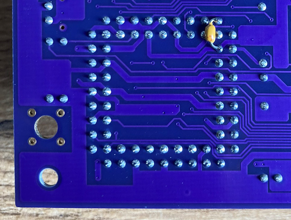
Backside position CXX (CAP CER 220 pF axial or 0805 SMD)

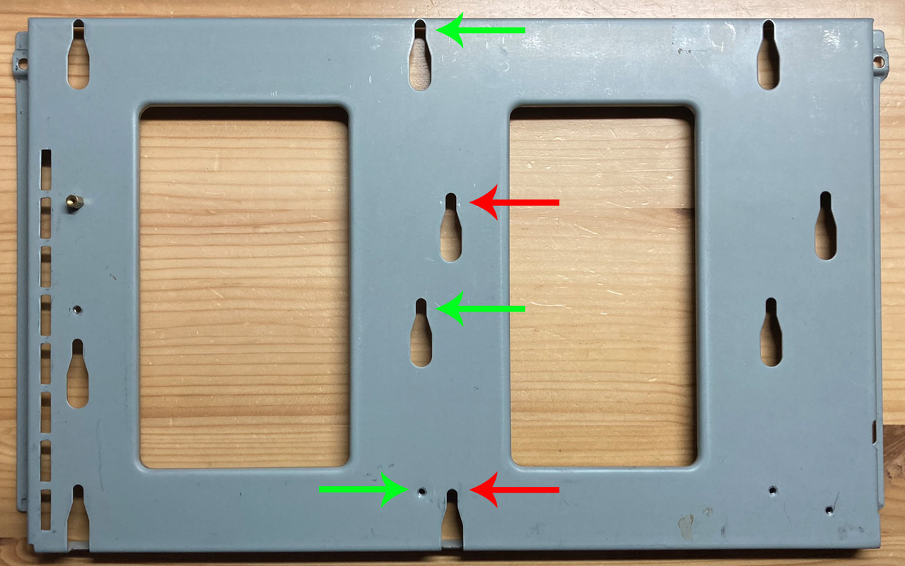
This board uses the mounting holes marked in green. Modern AT cases often only have the red marked holes.
The project is free for non-commercial reproduktion. Do not sell it on ebay or other platforms for profit. Do not make a closed source. Share your experiences and ideas with the community.


