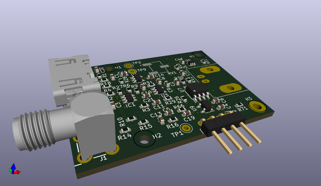
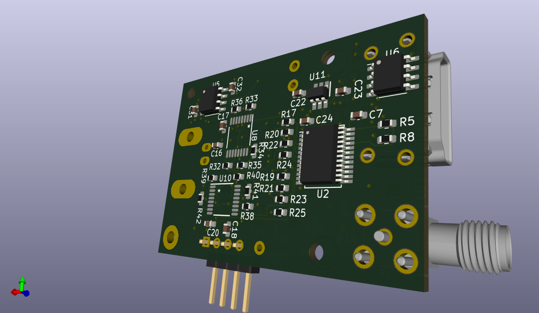
This board is physically small so it can be housed in an enclosure on a micromanipulator. The board input is a BNC connector which is compatible with glass microelectrode holders.
The input amplifier must have low capacitance to minimize the total filter from the capacitance and the microelectrode resistance. The first version has a fixed amplifier gain.
The Rev_b board modifications were designed and implemented by undergraduate student Jordan Haag. The board incorporates programmable gain and uses a low-noise voltage reference, REF3440, as the reference input to the offset adjust DAC. The low-noise reference improves the noise performance of the system.
The schematic is in the DOCS folder.
The second revision of this board was fabricated and assembled by JLCPCB.
Order #: Y13-3276043A
Assembly: SMT02402281623205-3276043A
Date: 2024/02/29
Certain parts are not directly available from LCSC and so were pre-ordered. Pre-order: 24AA025UID, OPA1641, DAC101C081CIMK/NOPB, TMUX6111PWR, TCA9555DBR, LP2981A-33DBVT, ADA4000-2ARZ-R7. Global sourcing: 3269W-1-103GLF, REF3440TIDBVR.
- A footprint for a capacitor should be included in parallel with the feedback gain resistors, for example R33, R34, R35, and R36. This limits the amplifier bandwidth. Currently we work around this omission by stacking a capacitor on top of the resistor. Issue (#4)
- U8,U10 (TMUX6111) and U11 (REF3440) were not assembled by JLCPCB and were lated added by hand.
This version addresses the following issues that occured with V1
- DAC reference noise: #5
- Negative capacitance connection: #3
- C8 causes oscillation: #2
- Incorrect BOM resistor values: #1
The digital COVG project uses the concept of one main data acquisition board connected to an FPGA. The main data acquisition board has multiple channels that extend to daughtercards. The connection to each daughtercard allows for low-latency control by connections to high-speed ADCs and DACs on the daq board. For COVG the daughtercards are the bath clamp; the guard clamp; the voltage clamp and I force; and the V1/V2. The connectivity to the daughtercard is generalized and will be the same for each.
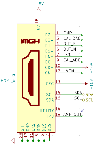
An HDMI-A cable is used for input and output signals that connect the bath clamp daughtercard to the DAQ board. The HDMI cable carries:
- power: +5V, +15V, -15V
- GND
- Analog outputs (to ADCs):
- OUT_P, OUT_N differential pair (x1) to 5 MSPS ADC
- single-ended out AMP_OUT, CAL_ADC both to individual channel of 1 MSPS ADC (ADS8686)
- Analog reference: VCM: buffered ADC common-mode voltage (nominal 2.5 V)
- Digital inputs (from DACs):
- CMD: (command signal) from 1 us settling time DAC (attenuated by x10 at board)
- CC: (capacitive compensation) from 1 us settling time DAC. AC coupled.
- CAL_DAC: from 5 us settling time DAC (DAC8050). Either voltage source or current source (Howland current pump), programmable on DAQ board
- Digital control (I2C): SDA, SCL (@ 3.3 V levels). Pull-ups are on DAQ board not on the daughtercards! The daughtercards use a TCA9555 I/O expander to generate many control signals from the I2C interface.
- Utiility grab-bag connected to test-point. Jumper on DAQ board to set to analog in, analog out or digital I/O.
| Pin | HDMI name | Generic Daughtercard | Bath clamp | Notes |
|---|---|---|---|---|
| 1 | Data2+ | fastDAC1 | CMD | ~1 us settling time |
| 2 | Data2 shield | Gnd | Gnd | |
| 3 | Data2- | Analog/GPIO1 | CAL_DAC | Analog input signal from DAC8050, 16 bit, 5us settle, 5 V supply |
| 4 | Data1+ | fastADC+ | IM_P | to AD7960/AD7961. Differential low-pass filter on DAQ board |
| 5 | Data1 shield | Gnd | Gnd | |
| 6 | Data1- | fastADC- | IM_N | to AD7960/AD7961. Differential low-pass filter on DAQ board |
| 7 | Data0+ | fastDAC2 | CC | ~1 us settling time |
| 8 | Data0 shield | Gnd | Gnd | |
| 9 | Data0- | Analog/GPIO2 | CAL_ADC | to ADS8686 1 MSPS, programmable PGA for range up to +/-10V |
| 10 | Clock+ | 15V | 15V | From a linear regulator on the DAQ board, 75 mA max per channel |
| 11 | Clock shield | Gnd | Gnd | |
| 12 | Clock- | VCM | VCM | buffered on DAQ board, nominal 2.5 V |
| 13 | CEC | -15V | -15V | From a linear regulator on the DAQ board, 75 mA max per channel |
| 14 | Reserved | open | open | Resistor jumper on DAQ board sets as analog in, analog out, or digital I/O (@ 3.3 V levels). Default stuffing option is to connect to the general purpose ADC (ADS8686). |
| 15 | SCL | SCL | SCL | I2C clock. Pull-up on main DAQ board, 3.3 V levels |
| 16 | SDA | SDA | SDA | I2C data. Pull-up on main DAQ board, 3.3 V levels |
| 17 | Gnd | Gnd | Gnd | |
| 18 | 5V | 5V | 5V | Power input from linear regulator, 200 mA max per channel (target) |
| 19 | HPD | Analog/GPIO3 | AMP_OUT | output to ADS8686 1 MSPS, programmable PGA |
Research reported in this repository was supported by the National Institute Of Neurological Disorders And Stroke of the National Institutes of Health under Award Number R15NS116907. The content is solely the responsibility of the authors and does not necessarily represent the official views of the National Institutes of Health.


