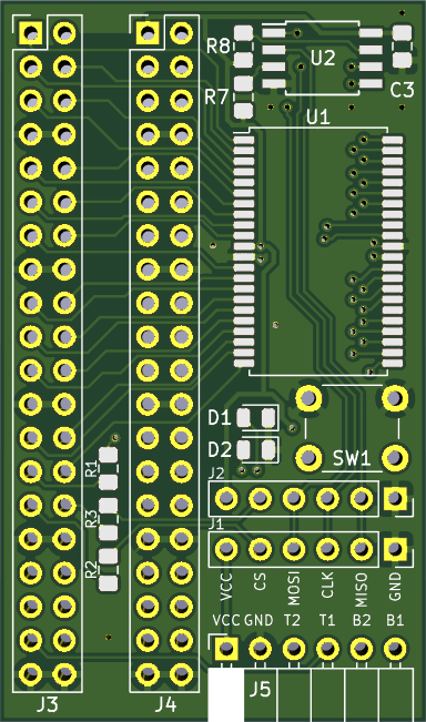
A PCB with 4 Mbit of SRAM, SPI-Flash, two LEDs, a button, SPI-connectors, and a single-row pmod-compatible connector for the Lattice HX8K Breakout Board. Connects to the headers J3 and J4 on the Lattice HX8K Breakout Board.
The board in its current state is difficult to operate in a stable manner. While signals to the SRAM-chip appear to be of decent quality, I've yet to achieve stable operation over extended periods of operation. This might be a matter of my SRAM-controller design within the FPGA, or an issue with the board design available here. Please be aware of this before considering deploying this design in your projects.
| Component | Description | Qty. |
|---|---|---|
| U1 | 4 MBit SRAM chip, 256Kx16, e.g. AS7C34098A, 10ns or faster recommended, TSOP-II 44 package | 1 |
| U2 | SPI-Flash, e.g. W25Q32JV, 8-Pin SOIC package | 1 |
| C1, C2, C3 | 100nF ceramic capacitor, 0805 package | 3 |
| D1, D2 | SMD LEDs, red, 0805 package | 2 |
| R1, R2, R3, R4, R5, R6, R7, R8 | resistors, 1K, 0805 package | 8 |
| R9 | optional pull-up for SW1, anything between 10K and 50K should be fine, 0805 package | 1 |
| R10, R11 | resistors for the LEDs, 510 Ohm, 0805 package (important: populate before J3 and J4, as R10 and R11 will become inaccessible) | 2 |
| SW1 | 6x6 mm push button, THT | 1 |
| J1, J2 | 1x6 female header, 2.54 mm pin spacing | 2 |
| J3, J4 | 2x20 male pin headers, 2.54 mm pin spacing (important: solder on top side, so pins head downwards towards FPGA board) | 2 |
| J5 | 1x6 female right-angled header, 2.54 mm pin spacing | 1 |
