Advanced Digital Systems
Caesar Cipher Digital System
I. Key components :
1. Keyboard A keyboard consists of a matrix of keys and an embedded microcontroller that monitors (i.e., scans) the activities of the keys and sends scan code accordingly. Three types of key activities are observed: ● When a key is pressed, the make code of the key is transmitted. ● When a key is released, the break code of the key is transmitted. ● When a key is held down continuously, a condition known as typematic, the make code is transmitted repeatedly at a specific rate. By default, a PS2 keyboard transmits the make code about every 100 ms after a key has been held down for 0.5 second. The make code of the main part of a PS2 keyboard is shown in Figure below. It is normally 1 byte wide and represented by two hexadecimal numbers. For example, the make code of the A key is IC.
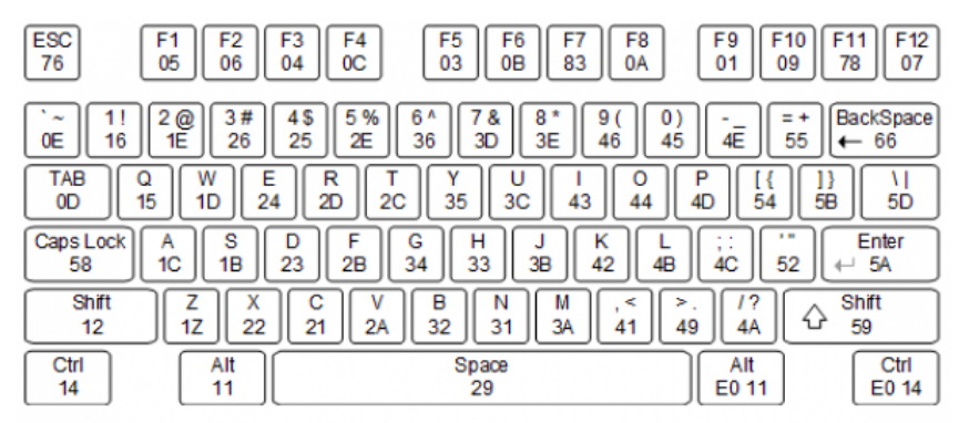 Figure 1: Keyboard scan codes set
Once powered, the keyboard goes through a self- initialization sequence. Upon completion, it is ready to communicate keyboard events over the PS/2 interface. Figure 2 illustrates the transaction format. Both clock and data signals are logic level high when inactive. The keyboard provides both the clock and data. The clock has a frequency between 10 kHz and 16.7 kHz (i.e. a 60-100us period). The data begins with a start bit (logic low), followed by one byte of data, a parity bit, and finally a stop bit (logic high). The data is sent LSB first. Each bit should be read on the falling edge of the clock signal. Once complete, both the clock and data signals return to logic level high.
 Figure 2: PS/2 Keyboard Transmission Timing Diagram
The data byte represents part of a keyboard scan code: either a make code (key press) or a
break code (key release). Three different sets of scan codes exist, however the vast majority of
keyboards use Scan Code Set 2, which is provided in Figure 1. A make code usually consists of
either one or two bytes.
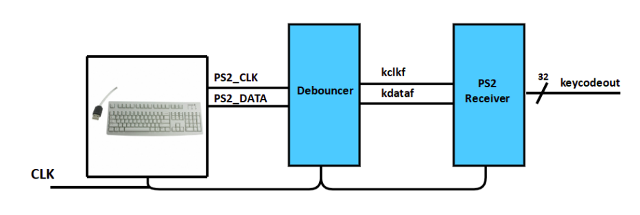
Figure 3 conceptually illustrates the PS/2 keyboard interface component’s architecture. The
clock and data signals from the keyboard are first synchronized and denounced. The resultant
internal PS/2 data signal is then serially loaded into a shift register on falling edges of the PS/
clock. An idle counter determines when the transaction is finished, defined by the PS/2 clock
remaining at a high logic level for 50us, i.e. longer than half of the worst-case PS/2 clock
period. Combinational error checking logic verifies the start bit, stop bit, and parity bit with the
data. When the PS/2 port is idle and the data is valid, the component outputs the received
PS/2 code and sets the datacur signal high to indicate that a new code is available on
the keycode bus. The code remains available on the bus until another code is received.
The datacur signal remains high until another PS/2 (datacur will be dataprev) transaction begins
(when a low PS/2_CLK signal clears the idle counter).
Figure 3: PS/2 Keyboard Interface Logic Architecture
2. VGA
A Video Graphics Array (VGA) is a standard type of connection for video devices such as
monitors and projectors. The VGA connector has 15 pins as shown in Figure 4, which is used to
determine colors, position of writing and written data.
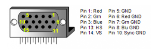 Figure 4: VGA connecter
The Nexys4 DDR board uses 14 FPGA signals to create a VGA port with 4 bits-per-color and the
two standard sync signals (HS – Horizontal Sync, and VS – Vertical Sync). A video controller
circuit must be created in the FPGA to drive the sync and color signals with the correct timing in
order to produce a working display system.
 Figure 5: VGA display controller block diagram
A VGA controller circuit, shown in Figure 5, decodes the output of a horizontal-sync counter
driven by the pixel clock to generate HS signal timings. This counter can be used to locate any
pixel location on a given row. Likewise, the output of a vertical-sync counter that increments
with each HS pulse can be used to generate VS signal timings. Also it can be used to locate any
given row. These two continually running counters can be used to form an address into video
RAM. No time relationship between the onset of the HS pulse and the onset of the VS pulse is
specified, so the counters can be arranged to easily form video RAM addresses, or to minimize
decoding logic for sync pulse generation.
3. Caesar Cipher The Caesar Cipher technique is one of the earliest and simplest methods of encryption technique. It is simply a type of substitution cipher, i.e., each letter of a given text is replaced by a letter with some fixed number of positions down the alphabet. For example with a shift of 1, A would be replaced by B, B would become C, and so on. The method is apparently named after Julius Caesar, who apparently used it to communicate with his officials. In order to cipher a given text we need an integer value, known as shift which indicates the number of positions each letter of the text has been moved down. Typically, this encryption can be represented using modular arithmetic by first transforming the letters into numbers, according to the scheme, A = 0, B = 1,..., Z = 25. Encryption of a letter by a shift n can be described mathematically as shown in Figure 6. In this project, we don’t need to convert the character to it’s alphabetical order since each character is represented in binary ASCII code, so we will apply these equations to the ascii code directly, and we will add / subtract 3 to each character code to find the third successor / predecessor letter as shown in the equations below.
En(x) = x + n; // n = 3
(Encryption Phase with shift n)
En(x) = x - n; // n = 3
(Decryption Phase with shift n)
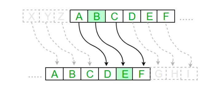 Figure 6: Caesar cipher
II. Top level diagram
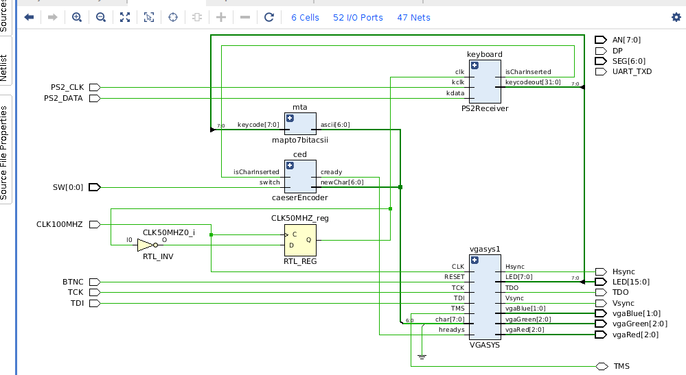
The diagram below explains this process flow of this project:

