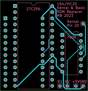
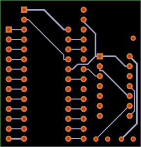
My VIC20's Basic ROM is kaput. So took the opportunity to design a simple PCB to allow both the basic ROM and the Kernal (this is how Commodore spell Kernel) ROM to be replaced with a single 27C256 (this is what I had - double what is needed).
The project is constructed in Kicad. The output files are generated in Gerber format.
The PCB replaces the Basic ROM and Kernal ROM. The PCB plugs in to the Basic ROM socket and also runs a single fly lead to Pin 20 of the Kernal ROM socket (with Kernal ROM completely removed).
A quad AND gate is used to control the output enable line of the EPROM and is also used to enable the additional banks on the EPROM when switched.
As the EPROM is twice the required size, this allows us to include two Basic ROMs and two Kernal ROMs in the EPROM. Address line 13 can then be switched to enable the second ROM.
Contacts are provided for two switches. The first switch switches Basic ROM between bank 1 and bank 2 and the second switches the Kernal ROM between bank 1 and 2.
The circuit simply achieves the following:
- Connects the appropriate pins from the Basic ROM to the EPROM to achieve like for like.
- Enables chip output if either the Basic or Kernal ROM is chip enabled. This is achieved using a single AND gate with BASIC ROM and Kernal ROM chip enable pins (high if not enabled) connected to the inputs.
- Sets address line 14 high if the Basic ROM is not chip enabled (therefore allowing the Kernal ROM to be included in the top 16k of the EPROM).
- Sets address line 13 high if the appropriate switch is selected. This is achieved using 2 AND gates. The first takes the input of switch 1 (high when switched) and the chip enable of the Kernal ROM. If the Kernal ROM C/E is high we assume the Basic ROM is enabled instead and therefore if the switch is high, we switch in address line 13 (14 should be low at this point). Note that it is possible for neither the Kernal or Basic ROM to be enabled and in this case the AND gate will incorrectly assume the Basic ROM is enabled however this is fine as in this case the EPROM output enable will be disabled (see item 2). The second AND gate takes the Basic ROM chip enable and Switch 2 (high on active) inputs. The output will enable if Kernal ROM is active and the switch is set. The output of both AND gates are joined and connected to address line 13.
The EPROM is segmented as follows:
- 0k-8k Basic ROM (bank 1) Address line 13 LOW; Address line 14 LOW
- 8k-16k Basic ROM (bank 2) Address line 13 HIGH; Address line 14 LOW
- 16k-24k Kernal ROM (bank 1) Address line 13 LOW; Address line 14 HIGH
- 24k-32k Kernal ROM (bank 2) Address line 13 HIGH; Address line 14 HIGH
The ROM configuration I have used is as follows:
- 0k-8k basic.901486-01
- 8k-16k basic.901486-01 (duplicated)
- 16k-24k kernal.901486-07
- 24k-32k JiffyDOS_VIC-20
A switch is connected between +5v and switch 2. Switch 1 is left disconnected.
2 x 20 contact (only need 12 contact by 20 is more common) Board-to-Board through hole straight pin headers. For example https://au.element14.com/amp-te-connectivity/2-826629-0/btb-conn-header-20pos-1row-2-54mm/dp/1580047 These are soldered to the 2 rows of 12 through-holes on the underside of the board and are used to plug in to the Basic ROM socket. Solder these first.
1 x 28 contact DIP 2.5mm x 15.24mm socket. The socket should slightly stand off the board to not interfere with the pin headers. For example https://au.element14.com/multicomp/2227mc-28-06-07-f1/socket-ic-dil-0-6-28way/dp/1103852 This soldered to the topside of the PCB for mounting the 27C256.
1 x SN74LS08n quad AND gate. For example https://au.element14.com/texas-instruments/sn74ls08n/logic-quad-2-inputgate-14dip/dp/3120526
2 x optional single pole miniature toggle switches (only single throw required) For example https://au.element14.com/e-switch/100sp1t1b1m1qeh/toggle-switch-spdt-5a-120vac-28vdc/dp/2522278 The switches are wired to B2 En (basic bank 2 enable) and K2 En (Kernal bank 2 enable)
1 x 10cm of wire to connext "Kernal Pin 20" contact to pin 20 of the Kernal ROM. Tin the end of the wire so it fits firmly into the socket.
1 x 27C256 EPROM (or compatible - eg AT28C256 will also work) I've used a write once compatible EPROM here.
Each switch is wired as follows:
- Center pin to EN, top pin to GND, bottom pin to +5V.
Note that the EN should be tied to GND on the PCB if the switch is not used.

