dsPIC33 4-Switch Buck-Boost Converter
- How to use this document
- Summary
- Related Collateral
- Quick-start Guide
- Control Method
- Converter State Machine Overview
- Plant Frequency Response Simulation with MPLAB® Mindi™
- Importing Plant Frequency Response into DCDT
This document is intended as a supplement to the user's guide. We recommend that the user's guide is studied before reading this document. The user's guide can be found here..
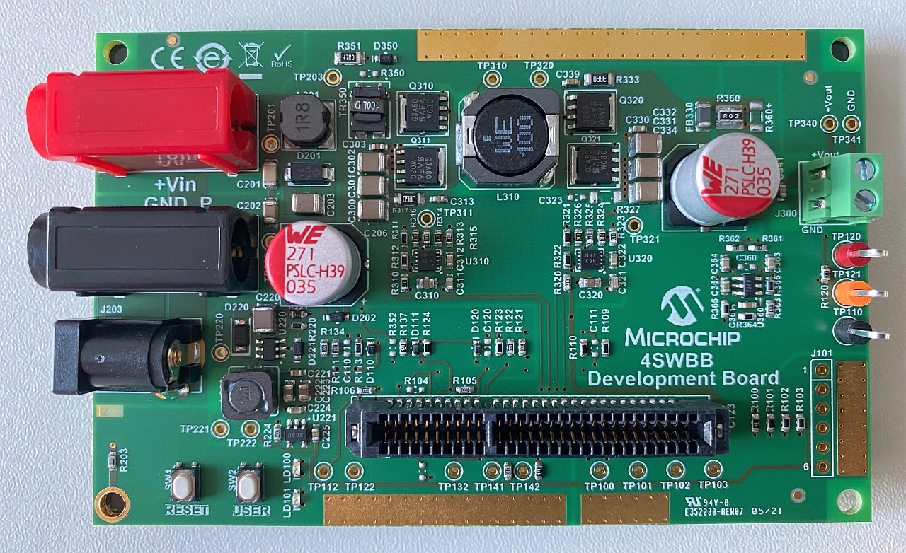
This solution demonstrates the implementation of a 4-switch buck-boost converter using average current mode control on the Four-Switch Buck-Boost Development Board (4SWBB). This power board is a generic development board for this topology that supports rapid prototyping and code development based on dsPIC33 devices. The board provides organized building blocks that include an input filter, power stage, AUX supply, mating socket for Microchip’s newest Digital Power Plug-In Modules (DP-PIMs), Human Machine Interface (HMI) and test points. The electrical characteristics are applicable to automotive requirements and can be used for these applications as well. For example, input power can be a standard 12V vehicle power rail and operate within the automotive ambient temperature range. A mating socket for dsPIC33 Plug-In Modules allows the system to be evaluated with different controllers. The pin-out is compatible for EP, CK and CH dsPIC® DSC DP PIMs.
The associated firmware uses average current mode control to regulate the output voltage. The input voltage range is 8V to 18V, and the output voltage range is 5V to 20V. It can run without external cooling up to 20W and 2A at the output.
The firmware also includes a scheduler to allow the user to easily add their own housekeeping functions. In our example code, the scheduler executes drivers for the Human Machine Interface (HMI) and for communication with the Board Power Visualizer GUI.
The related documentation can be found on the appropriate product website
- Four-Switch Buck-Boost Development Board
- dsPIC33CK256MP508 Family Data Sheet
- dsPIC33CK256MP508 Family Silicon Errata and Data Sheet Clarification
Please always check for the latest data sheets on the respective product websites:
- Power Board Visualizer GUI
- MPLAB® X IDE v5.45
- MPLAB® XC16 Compiler v1.61
- Microchip Code Configurator v4.0.2
- Digital Compensator Design Tool
- MPLAB® Mindi™ Simulator
- Four-Switch Buck-Boost Development Board, Part-No. EV44M28A
- dsPIC33CK256MP506 Digital Power PIM, Part-No. MA330048
In this section, we describe step by step how to run the firmware on the power board. We also describe how to interface with the board power visualizer GUI.
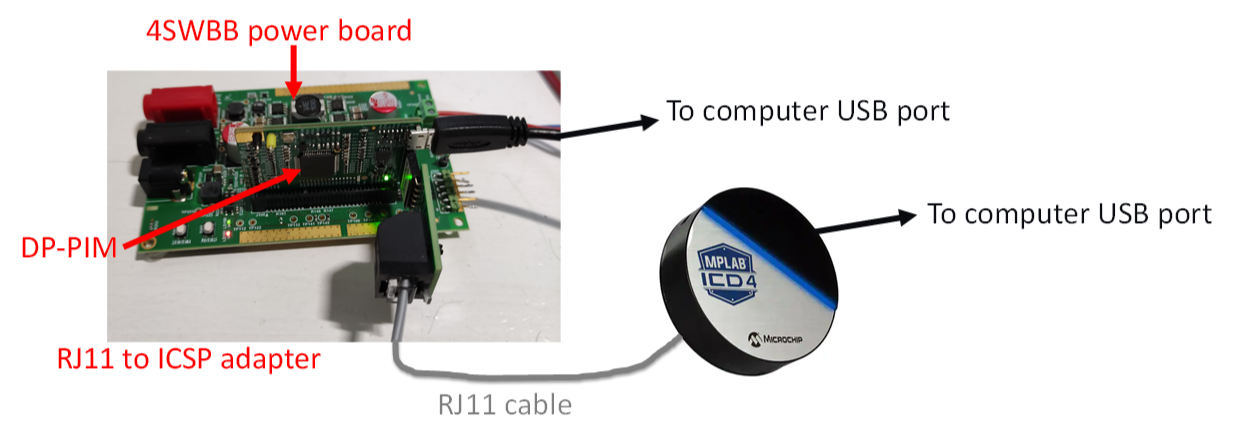
Connect the DP-PIM to the power board. Then connect the ICD4 debugger to the 6-pin header on the DP-PIM via the RJ11 cable and the RJ11 to ICSP adapter. Finally, connect a USB cable between the micro-USB port on the top-right of the DP-PIM and your computer - for this you will require a type A to micro-USB type B cable.
Connections from DP-PIM and power board to computer
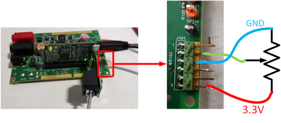
The firmware provides the capability for a potentiometer to provide the output voltage reference. We recommend using the facility the first time you bring up the board. The potentiometer needs to be connected to the 6-pin header on the edge of the power board, as shown below.
Connecting a potentiometer to the power board, to provide the voltage set-point There is an 8:1 resistive divider on the power board between the converter output terminals and the dsPIC pin at which the output voltage is sensed at. Hence, if the potentiometer is used to provide the voltage loop reference, in closed loop operation the output voltage = (Voltage at pin 2 of header) * 8.
At start-up, the firmware detects if a potentiometer is present, and if so, uses the voltage on pin 2 of the header as the reference for the voltage loop compensator. If no potentiometer is sensed, then the default set-point is fixed to get 12V at the output terminals.
For first board bring up, set the potentiometer wiper to get the lowest possible voltage on pin 2 of the header.
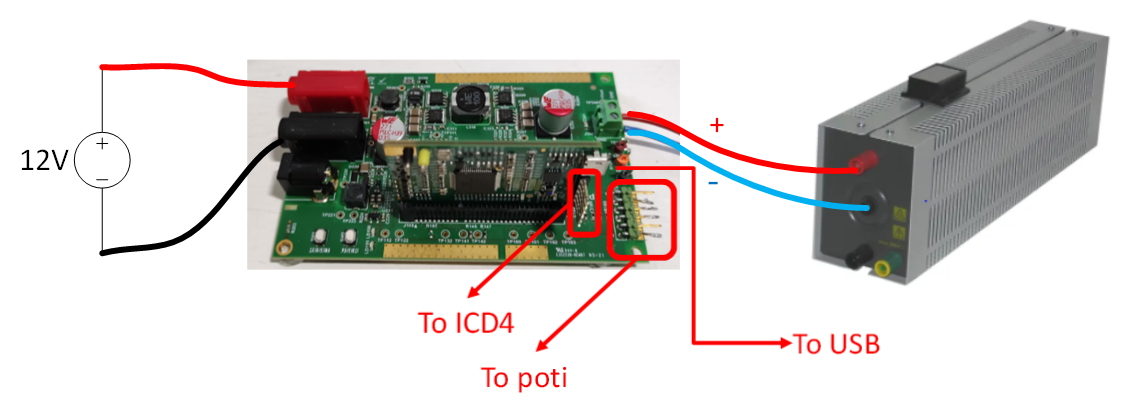
Next, connect a voltage source to the input terminals and a load to the output terminals as shown below. For first board bring-up, set Vin=12V and use a resistive load of approximately 30R. The output voltage can be probed at test point TP340, which is located at the top right of the board. Once the converter is up and running, you can change these values.
Connecting a source and a load to the power board Next, follow the instructions in the user’s guide to program the dsPIC via MPLABx.
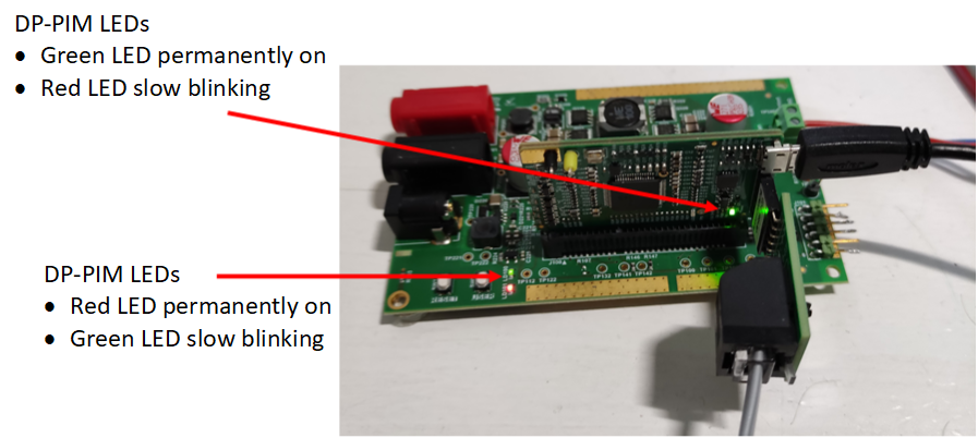
At this point, the code should be running on the dsPIC without any input voltage or load. You should now check the status LEDs on the power board and DP-PIM (for more information on the status LEDs, please refer to the user’s guide).
Status LEDs with firmware running
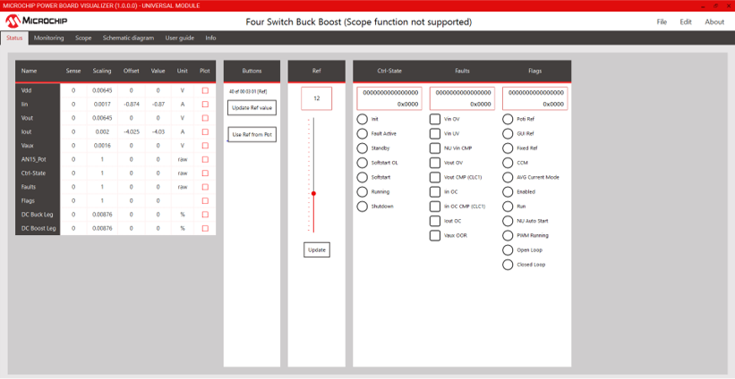
Open board power visualizer on your computer. On the window that appears, click "Open Project", and then navigate to the "gui" folder (the "gui" folder is at the same level as this README.md file). Select "4SWBB", and the window below will open.
Board power visualizer window for 4SWBB
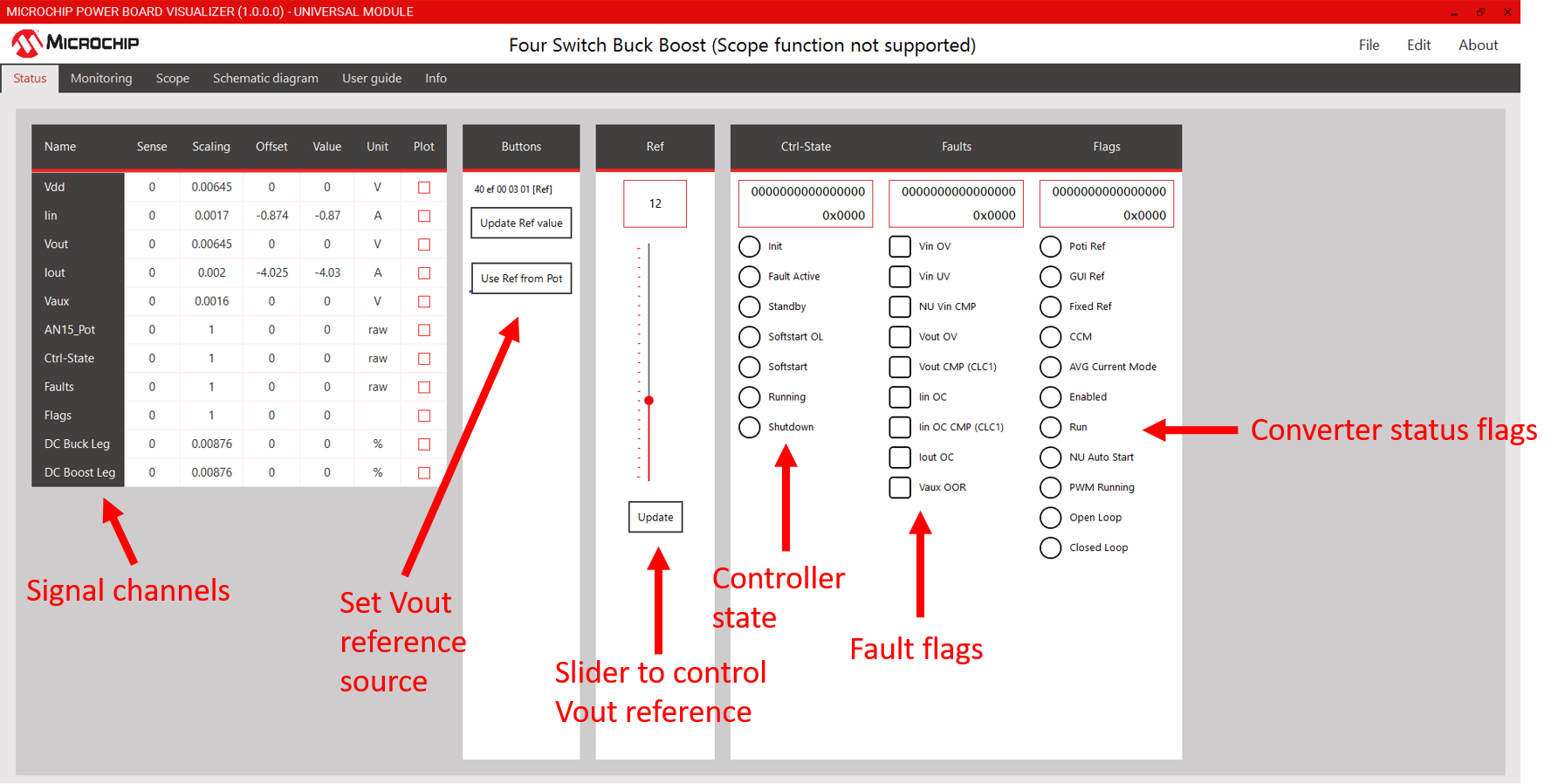
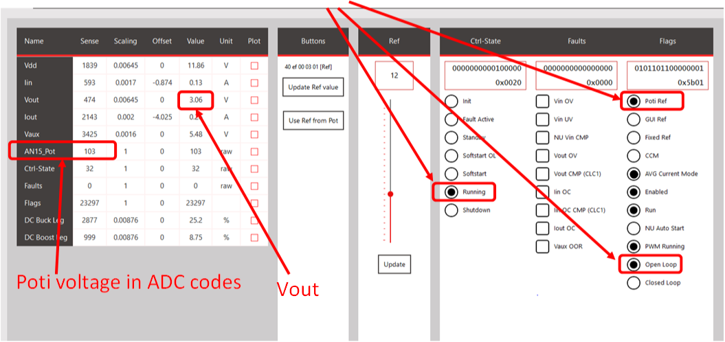
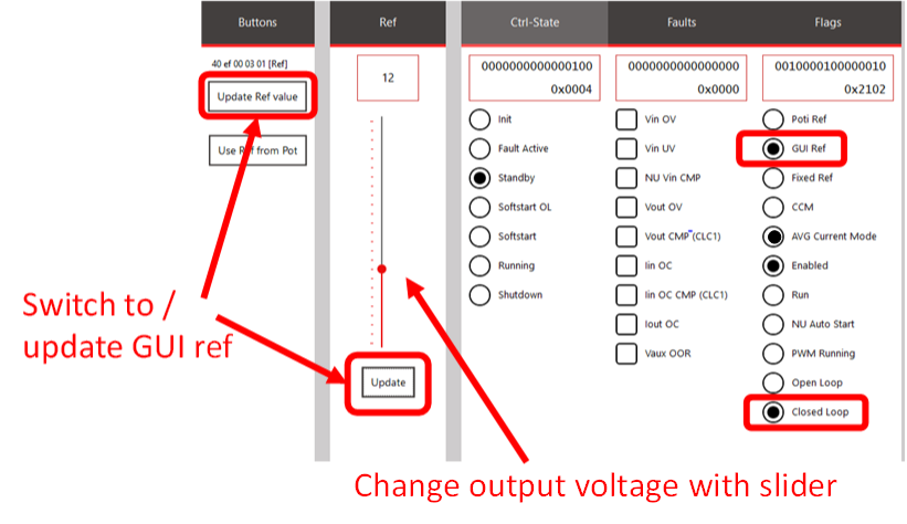
More information about the items in the status window is shown below. On the left are the "signal" channels, to the right there are buttons and a slider to control the output voltage reference source and value. On the right, the controller state, fault flags and status flags are shown.
Board power visualizer status window There are a number of other tabs on the top of the screen, you can click on these to find out more, they are pretty self-explanatory hence we don't go into much detail on tabs in this document.
Board power visualizer tabs
Now you need to pair the GUI with the firmware running on the dsPIC. To do this, click on the "COM?" button, select the port and speed (the speed should default to the correct value of 115200), then click on the "Enable" button.
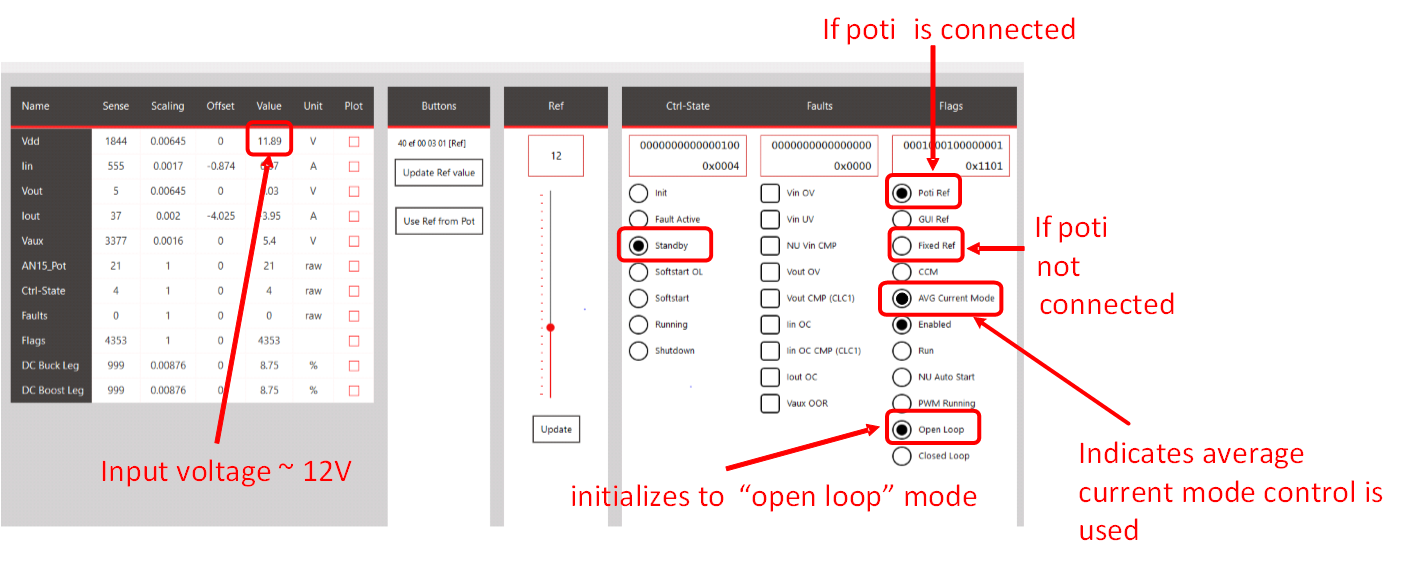
If the communications channel is working, you should see the "Communications status" button on the bottom left of the status window flashing alternately green and red. The status window should show around 12V on Vdd, the converter state should be "standby" and the "Open loop" flag should be asserted. The "AVG current Mode" flag should also be asserted, indicating that this firmware uses average current mode control.
GUI status window at start-up
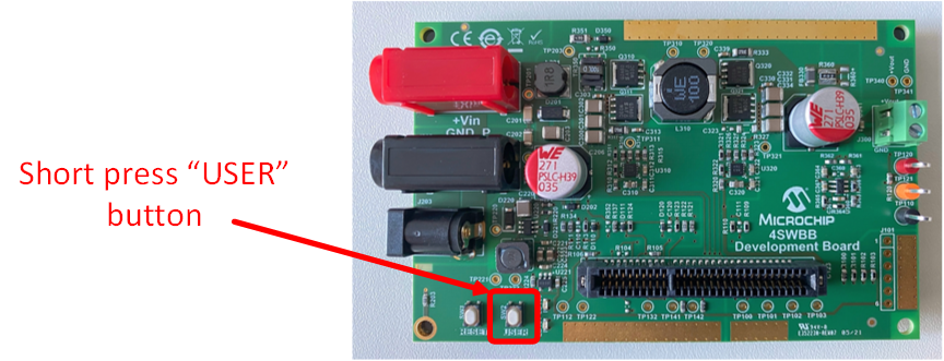
To start running the converter, short press the "USER" button on the power board.
Starting the converter The converter is now running "open loop". This means that the duty cycle is set directly based on the potentiometer voltage. The voltage loop compensator output is ignored in open loop mode.
At this point
- The green LED on the power board should be permanently on.
- The Red LED on the power board should be slow blinking.
Going back to the GUI screen, you should see the following:
GUI status window with converter running open loop, with poti reference To change the output voltage, move the poti wiper.
- Short press the "USER" button on the power board.
- This turns off the converter.
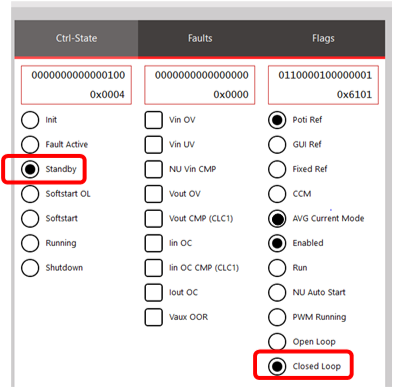
- "Ctrl-State" on the GUI should be "Standby".
- Long press the "USER" button: this changes to "closed loop" mode.
- Poti voltage provides reference to voltage loop compensator.
- Voltage loop compensator provides reference to current loop compensator.
- Current loop Compensator drives the duty cycle.
- Set potentiometer wiper to get minimum voltage on pin 2 of 6 pin header.
GUI status window with converter in standby, closed loop mode
- Short press the "USER" button on the power board.
- This turns on the converter.
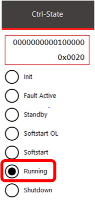
- "Ctrl-State" on the GUI should be "Running".
GUI status window with converter running in closed loop mode
- Observe the LEDs on the power board.
- Green LED should be permanently on.
- Red LED should be off.
The converter is now running in closed loop mode. This means that the potentiometer output is providing the reference to the compensator, and the output of the compensator drives the duty cycle.
Move the potentiometer wiper to change the voltage loop reference and thus the output voltage.
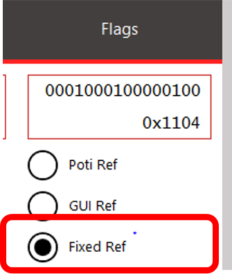
To run the firmware with a fixed internal reference, disconnect the potentiometer from the power board and re-start the firmware. At start-up, the firmware checks for the presence of the potentiometer. If the firmware determines that no potentiometer is connected, it used a fixed internal reference that corresponds to an output voltage of 12V. In this case, you will see that the "Fixed Ref" flag will be on.
Fixed Ref flag in GUI status window
To run closed-loop with a fixed reference:
- Long press "USER" button to change from open loop mode to closed loop mode.
- Short press "USER" button to run converter.
At this point, there should be 12V at the output. You can short-press the "USER" button to turn on/off the converter.
[back to top]
Configure the converter to run in closed loop mode. To use the GUI programmable reference, either click on the "Update Ref value" button on the GUI or click on the "Update" button on the slider. You can select the output voltage using the slider. The "GUI Ref" flag should be on when the GUI reference is active.
Using GUI output voltage reference
At this point, you can try different combinations of input voltages, output voltages and loads. Note that the converter can operate safely to a max output power of 20W, and max output load current of 2A.
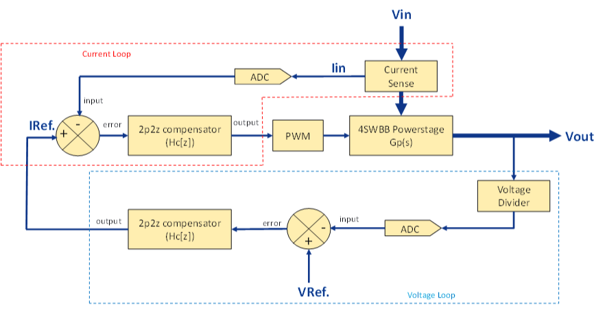
This version of the 4-switch buck-boost firmware uses Average Current Mode Control (ACMC).
In Average Current Mode Control the current reference (Iref) is generated by the outer voltage loop is set to be equal to the inductor current average. The "error" of the inner current loop passed through a 2 pole 2 zero (2P2Z) digital compensator. The output of the compensator is an integer that is proportional to the duty cycle, and this drives the pulse width modulator (PWM).
Essentially, the outer voltage loop sets the demand for the inner current loop so as to ensure that the charge removed from the output of the converter by the load is replenished at the same rate, so as the output voltage of the converter remains constant.
Average Current Mode Control
Note that the input current, which is sensed by the current transformer, is used as an input to the inner current loop.
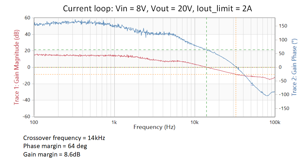
The frequency response of the (inner) current loop is shown below. The output current is limited to 2A in the firmware. For this measurement, the load is increased until the current limit is reached and Vout drops below 20V, this way the voltage loop is saturated and the current loop is in control.
Current loop frequency response
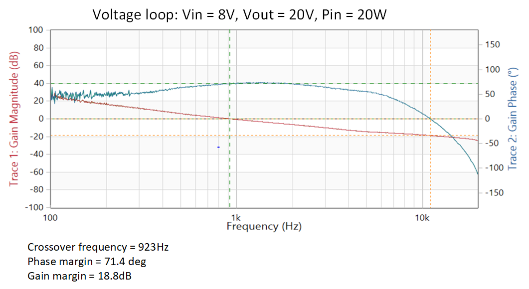
The frequency response of the (outer) voltage loop is shown below. The load is set so the input power is 20W.
Voltage loop frequency response
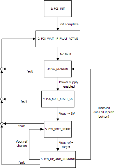
Some supplementary information on the converter state machine is given here. The converter state machine is run every 100us.
A brief description of each state is given in this section.
Converter state machine
- The PWM is initialized
- the PWM outputs are disabled but the PWM modules are running internally to trigger the ADC ISR.
- This is important as all signal measurements are based upon the ADC ISR.
- The fault handler is called every 100us, just before the state machine is executed.
- The fault counters for Vin under-voltage and over-voltage are set.
- Done here to enable Vin faults when auxiliary power is driven via USB connected to the DP-PIM.
- Stays here until all fault conditions are cleared.
- PWM is active, and the control mode (open loop or closed loop) is saved.
- Force switch to open loop mode
- means that current loop compensator does not drive the duty cycle.
- instead, the voltage loop demand directly drives the duty cycle.
- At this point, the voltage loop demand is set to 0, which corresponds to minimum duty cycle.
- Voltage loop demand, and hence Duty cycle, is increased linearly until Vout >= 3V.
- The saved control mode (open or closed loop) from state 3 is then restored.
- Voltage compensator initialized with pre-loaded value for controller output.
- Ensures a smooth start to the soft-start ramp.
- Voltage loop reference ramped linearly to give a fixed soft-start time under all conditions.
- Converter is running, and conditions based on flags are checked.
- Faults and HMI inputs can cause state change, depending on converter status.
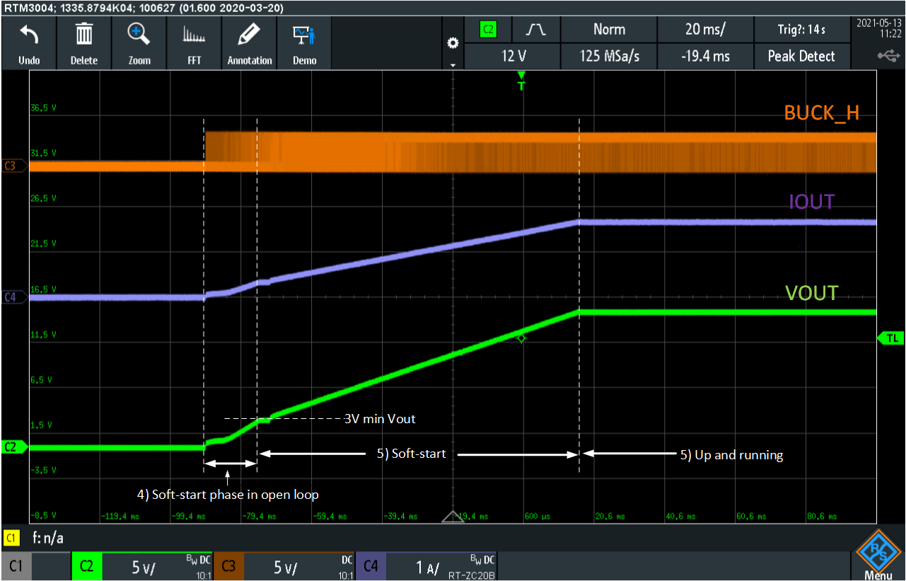
Additional information on the start-up characteristic is shown below.
Start-up characteristic We start off in open loop mode with minimum duty cycle: this means that the duty cycle is directly proportional to the voltage loop reference (the current loop compensator output is ignored). The voltage loop reference, and hence duty cycle, is slowly increased until the output voltage reaches 3V. When Vout >= 3V, the duty cycle is saved and used as the new buck minimum duty cycle. The converter then switches to closed loop mode and the voltage loop reference is ramped linearly until it hits its target value.
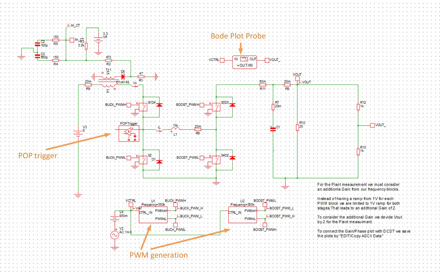
Mindi™ is the Microchip-branded demo version of Simplis/SiMetrix. It supports the common features of the Simplis standard license but limits the number of circuit nodes. A model of the 4SWBB plant is available with this deployment. To open the file in Mindi, select File -> Open, and navigate to 4swbb_01_using_generic_PWM_with_ACanalysis.wxsch.
Plant model in Simplis The model is setup to simulate the frequency response of the plant at a particular DC operating point.
The output of the PWM generation blocks on the bottom of the Mindi file generate a steady-state duty cycle (controlled by the DC source V4) superimposed with a small amount of AC jitter (controlled by the AC source V2). During the frequency response analysis, the frequency of the AC source V2 is swept from 100Hz to 200kHz.
By default, the input voltage is set to 8V and the duty is set to get an output voltage of 20V. R10 (the load resistor) is set to 20R so as the output power is 20W. These values can be changed to simulate the response at different operating points.
The POP (Periodic Operating Point) trigger is required to tell the simulator when each switching cycle starts, hence it needs to be placed on an appropriate node - here it is placed on the buck switching node.
The bode plot probes measure the gain and phase of the plant frequency response, both for the current and voltage.
To check the simulator settings, select Simulator -> Choose Analysis.
To run the simulation, select Simulator -> Run Schematic.
This Mindi schematic has been setup so as the simulated and measured plant gain have the same magnitude.
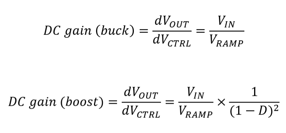
The plant DC gain of buck and boost converters in CCM is given by the following equations:
DC gain of buck and boost in CCM
The response to a disturbance is measured from the plant input - which is the modulator input VCTRL in our Mindi schematic, to the output terminals of the converter. The DC gain as defined in the equations at the start of this section is the magnitude of the disturbance as measured at the plant output divided by the magnitude of the disturbance as measured at the modulator input, at frequencies just above DC.
Vramp is defined as the peak to peak voltage of the sawtooth ramp in the modulator.
The two complementary PWM blocks on the bottom of the schematic generate the PWM switching signals. Internally, they use a sawtooth ramp to generate the PWM signals.
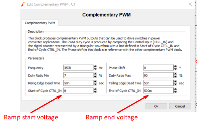
Buck PWM generator block settings Above we show the settings for the Complementary PWM block for the two buck switches. The ramp starts at 0V and ends at 0.5V, hence Vramp = 0.5V.
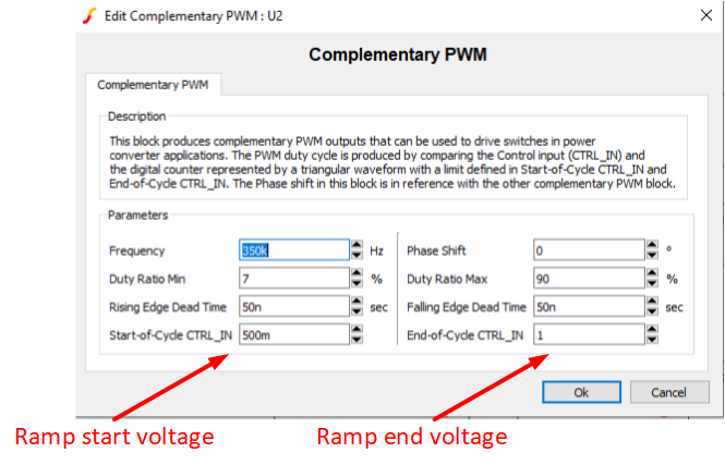
For the PWM generator for the boost switches, we show the settings below. The ramp start voltage = 0.5V, and stop voltage = 1V, hence Vramp = 0.5V, like for the buck converter.
Boost PWM generator block settings
We set the ramp magnitudes so as Mindi plant simulation matches the real plant measurements. If the open loop demand is less than 50%, the buck leg is active (duty changes with demand) and the boost leg runs at minimum duty cycle. For open loop demands greater than 50%, the buck leg runs at maximum duty and the boost leg is active.
So in our Mindi schematic, if V4 < 0.5V: the buck leg is active and the boost runs at min duty, and if V4 > 0.5V: the boost leg is active and the buck leg runs at max duty.
Because Vramp = 0.5V, the DC gains as given by the equations at the start of this section will be a factor of 2 greater than they will be in the measured result (as Vramp is in the denominator of the DC gain calculation for both the buck and the boost equations). This is why the output of the AC probe on the top right of our Mindi schematic is tied to the VOUT_ node and not directly to the converter output terminals (that is, the VOUT node). The VOUT_ node is the output voltage divided by 2. Thus, the gain of the plant measurements and Mindi simulations match pretty accurately.
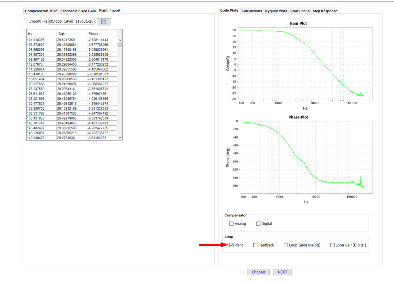
The Digital Compensator Design Tool (DCDT) helps power supply designers by simplifying the overall process of determining the digital compensator coefficients and analyzing the control system performance. The DCDT incorporates all feedback gains and delays to provide the most accurate model of the control system. Measurements of the plant frequency response can be imported into DCDT to help with the process of compensator design.
As an example, we have included a such a plant measurement taken using this development board, at Vin = 8V and Vout = 20V. The data needs to be in a .csv file. This file can be found in the directory "plant" and is called "BodePlant Vin 8V Vout 20V 20W.csv".
To import this data into DCDT, open MPLABx, then click Tools -> Embedded -> Digital Compensator Design Tool.
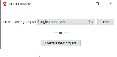
In the window that appears, select "Single-Loop: vmc" and then click "Open".
DCDT window In the next window, click "Plant"
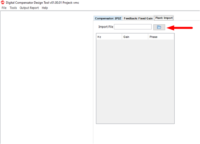
Plant selection in DCDT Then click "Chooser" on the bottom right of the window Then click "Import". Then import the file, clicking on the icon as shown below, and navigating to the "plant" directory, then selecting the file "BodePlant Vin 8V Vout 20V 20W.csv"
Importing plant measurements into DCDT
You can plot the plant gain and phase measurements in DCDT by checking the "plant" checkbox as shown below. The plant measurement can now be used to help you to design your compensator to achieve the performance that you require.
Plotting imported plant measurements
© 2021, Microchip Technology Inc.

