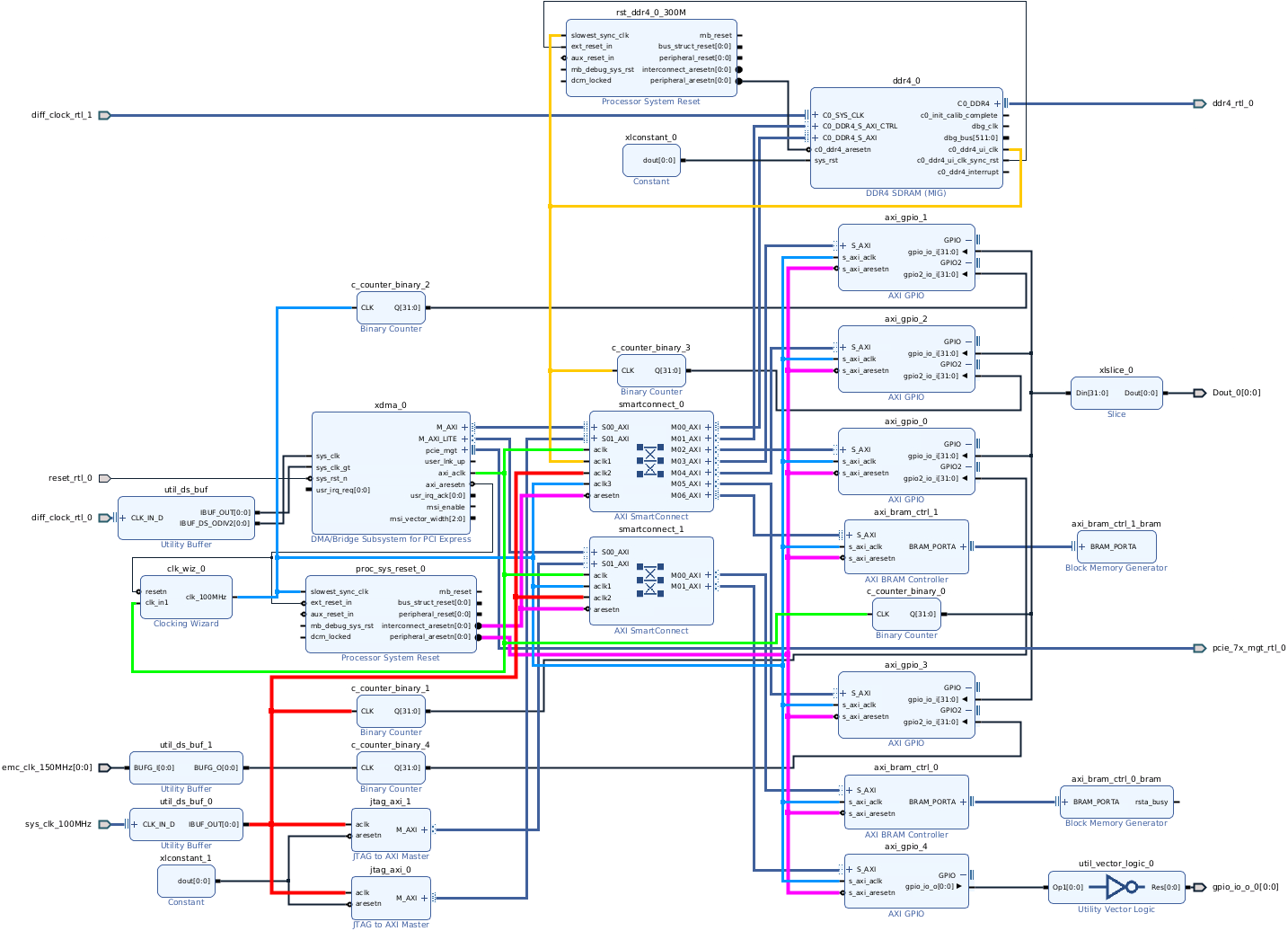
This is a Vivado 2023.2 starter project for the XCKU15P FPGA on the Innova-2 MNV303212A-ADIT/MNV303212A-ADAT. It is a superset of the innova2_xdma_demo project that adds a DDR4 controller for the 4GB of ECC DDR4 on the MNV303212A-ADIT/MNV303212A-ADAT.
Refer to the innova2_flex_xcku15p_notes project for instructions on setting up an Innova-2 system with all drivers including Xilinx's PCIe XDMA Drivers.
Refer to this tutorial for detailed instructions on generating a similar project from scratch.
There is also a version for the 8GB MNV303212A-ADLT variant available.
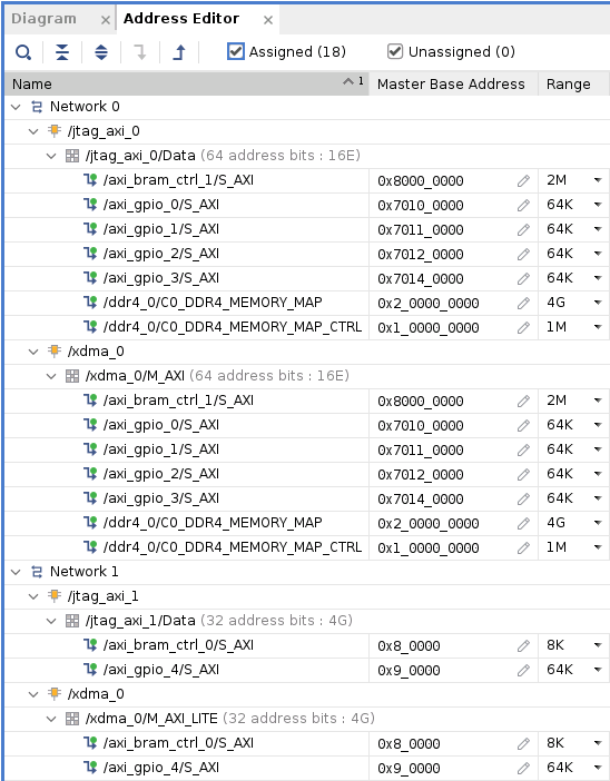
| Block | Address (Hex) | Size |
|---|---|---|
M_AXI BRAM_CTRL_0 |
0x80000000 | 2M |
M_AXI GPIO_0 |
0x70100000 | 64K |
M_AXI GPIO_1 |
0x70110000 | 64K |
M_AXI GPIO_2 |
0x70120000 | 64K |
M_AXI GPIO_4 |
0x70140000 | 64K |
M_AXI DDR4_0 |
0x200000000 | 4G |
M_AXI DDR4_CTRL_0 |
0x70200000 | 1M |
M_AXI_LITE BRAM_CTRL_1 |
0x00080000 | 8K |
M_AXI_LITE GPIO_3 |
0x00090000 | 64K |
- Program the Design into the XCKU15P Configuration Memory
- Testing the Design
- Recreating the Design in Vivado
- Block Design Customization Options
Refer to the innova2_flex_xcku15p_notes project's instructions on Loading a User Image. Binary Memory Configuration Bitstream Files are included in this project's Releases.
wget https://github.com/mwrnd/innova2_4gb_adit_xdma_ddr4_demo/releases/download/v0.1/innova2_4gb_adit_xdma_ddr4_demo_bitstream.zip
unzip innova2_4gb_adit_xdma_ddr4_demo_bitstream.zip
md5sum *bin
echo 69a8e6166fe713dca1c26d1398603282 should be md5sum of innova2_4gb_adit_xdma_ddr4_demo_primary.bin
echo 79e61b791d2246782e52ddcd926b2e5a should be md5sum of innova2_4gb_adit_xdma_ddr4_demo_secondary.bin
echo dc47755e2e08a9a8fc3a0a09e769cb3a should be md5sum of xdma_wrapper.bit
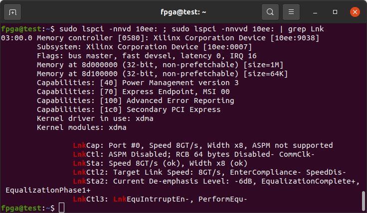
After programming the bitstream and rebooting, the design should show up as Memory controller: Xilinx Corporation Device 9038. It shows up at PCIe Bus Address 03:00 for me.
lspci -d 10ee:
The following lspci commands list all Mellanox and Xilinx devices and show their relation.
lspci -nn | grep "Mellanox\|Xilinx"
lspci -tv | grep "0000\|Mellanox\|Xilinx"
The FPGA is attached to a PCIe Bridge (02:08.0), as are the two Ethernet Controllers (02:10.0).
01:00.0 PCI bridge [0604]: Mellanox Technologies MT28800 Family [ConnectX-5 PCIe Bridge] [15b3:1974]
02:08.0 PCI bridge [0604]: Mellanox Technologies MT28800 Family [ConnectX-5 PCIe Bridge] [15b3:1974]
02:10.0 PCI bridge [0604]: Mellanox Technologies MT28800 Family [ConnectX-5 PCIe Bridge] [15b3:1974]
03:00.0 Memory controller [0580]: Xilinx Corporation Device [10ee:9038]
04:00.0 Ethernet controller [0200]: Mellanox Technologies MT27800 Family [ConnectX-5] [15b3:1017]
04:00.1 Ethernet controller [0200]: Mellanox Technologies MT27800 Family [ConnectX-5] [15b3:1017]

-[0]-+-00.0 Intel Corporation Device 3e0f
     +-1d.0-[01-04]----00.0-[02-04]--+-08.0-[03]----00.0 Xilinx Corporation Device 9038
     |                               \-10.0-[04]--+-00.0 Mellanox Technologies MT27800 Family [ConnectX-5]
     |                                            \-00.1 Mellanox Technologies MT27800 Family [ConnectX-5]
The current PCIe Link status is useful. Note this is the FPGA to ConnectX-5 PCIe Bridge link.
sudo lspci -nnvd 10ee: ; sudo lspci -nnvvd 10ee: | grep Lnk
dmesg | grep -i xdma provides details on how Xilinx's PCIe XDMA driver has loaded.
The XDMA driver from dma_ip_drivers creates character device files for access to an AXI Bus. For DMA transfers to M_AXI blocks, /dev/xdma0_h2c_0 is Write-Only and /dev/xdma0_c2h_0 is Read-Only. To read from an AXI Block at address 0x12345600 you would read from address 0x12345600 of the /dev/xdma0_c2h_0 (Card-to-Host) file. To write you would write to the appropriate address of the /dev/xdma0_h2c_0 (Host-to-Card) file. For single word (32-Bit) register-like reads and writes to M_AXI_LITE blocks, /dev/xdma0_user is Read-Write.
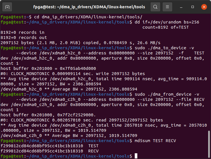
The commands below generate 2MB of random data, then send it to a URAM Block (0x80000000) in the XCKU15P, then read it back and confirm the data is identical.
cd dma_ip_drivers/XDMA/linux-kernel/tools/
dd if=/dev/urandom bs=256 count=8192 of=TEST
sudo ./dma_to_device   --verbose --device /dev/xdma0_h2c_0 --address 0x80000000 --size 2097152  -f    TEST
sudo ./dma_from_device --verbose --device /dev/xdma0_c2h_0 --address 0x80000000 --size 2097152 --file RECV
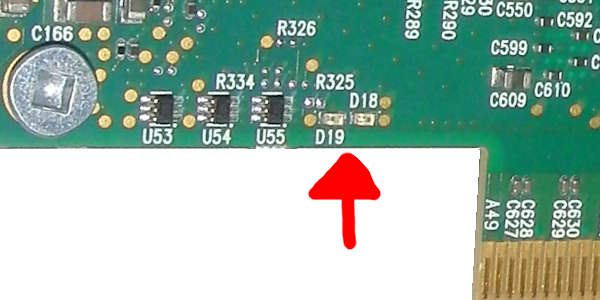
md5sum TEST RECVThe design includes an AXI GPIO block to control Pin B6, the D18 LED on the back of the Innova-2. The LED control is inverted on the board so the design includes a signal inverter. The LED can be turned on by writing a 0x01 to the GPIO_DATA Register. Only a single bit is enabled in the port so excess bit writes are ignored. No direction control writes are necessary as the port is set up for output-only (the GPIO_TRI Direction Control Register is fixed at 0xffffffff).
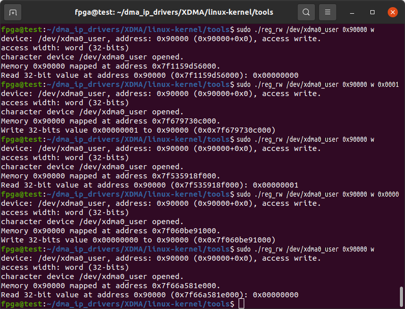
The LED GPIO Block is connected to the M_AXI_LITE port so access to it is via 32-bit=1-word reads and writes to the /dev/xdma0_user file using the reg_rw utility from dma_ip_drivers. The commands below should turn on then turn off the D18 LED in between reads of the GPIO register.
cd dma_ip_drivers/XDMA/linux-kernel/tools/
sudo ./reg_rw /dev/xdma0_user 0x90000 w
sudo ./reg_rw /dev/xdma0_user 0x90000 w 0x0001
sudo ./reg_rw /dev/xdma0_user 0x90000 w
sudo ./reg_rw /dev/xdma0_user 0x90000 w 0x0000
sudo ./reg_rw /dev/xdma0_user 0x90000 wThe DDR4 Controller prevents data reads from uninitialized memory. DDR4 must first be written before it can be read.
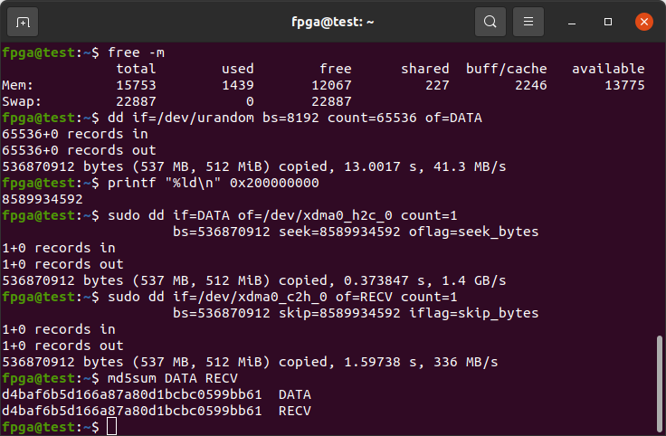
Your system must have enough free memory to test DDR4 DMA transfers. Run free -m to determine how much RAM you have available and keep the amount of data to transfer below that. The commands below generate 512MB of random data then transfer it to and from the Innova-2. The address of the DDR4 is 0x200000000 as noted earlier.
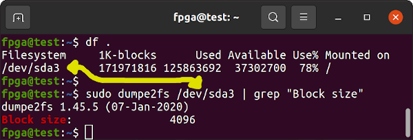
The dd command is used to generate a file (of=DATA) from pseudo-random data (if=/dev/urandom). The value for Block Size (bs) will be multiplied by the value for count to produce the size in bytes of the output file. For example, 8192*65536=536870912=0x20000000=512MiB. Use a block size (bs=) that is a multiple of your drive's block size. df . informs you on which drive your current directory is located. dumpe2fs will tell you the drive's block size.
df .
sudo dumpe2fs /dev/sda3 | grep "Block size"
To test the full 4GB of memory you can increment the address by the data size enough times that all 4Gib = 4294967296 = 0x100000000 has been tested.
If you have 4GB+ of free memory space, generate 4GB of random data with the dd command options bs=8192 count=524288 and test the DDR4 in one go.
dd uses decimal numbers. Convert from hexadecimal using printf.
If checksums do not match, vbindiff DATA RECV can be used to determine differences between the sent and received data and the failing address locations.
Note that data is loaded from your system drive into memory then sent to the Innova-2 DDR4 over PCIe DMA. Likewise it is loaded from the Innova-2's DDR4 into system RAM, then onto disk. The wall time of these functions can therefore be significantly longer than the DMA Memory-to-Memory over PCIe transfer time.
free -m
dd if=/dev/urandom bs=8192 count=65536 of=DATA
printf "%ld\n" 0x200000000
sudo dd if=DATA of=/dev/xdma0_h2c_0 count=1 bs=536870912 seek=8589934592 oflag=seek_bytes
sudo dd if=/dev/xdma0_c2h_0 of=RECV count=1 bs=536870912 skip=8589934592 iflag=skip_bytes
md5sum DATA RECV
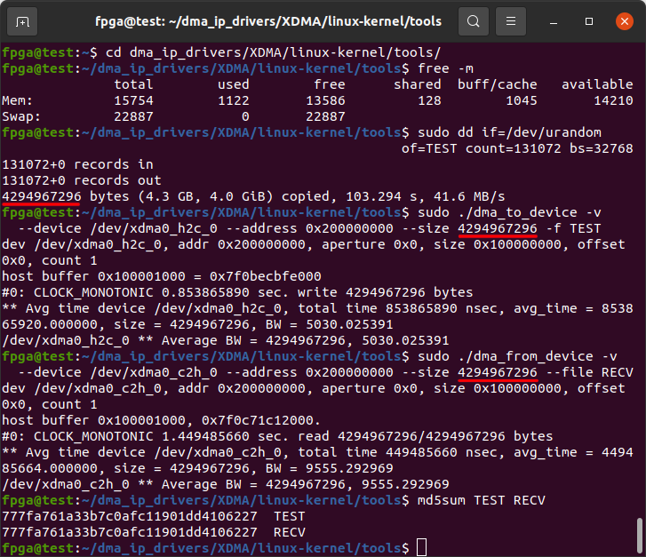
The tools from dma_ip_drivers can also be used to run a full memory test:
cd dma_ip_drivers/XDMA/linux-kernel/tools
free -m
dd if=/dev/urandom bs=32768 count=131072 of=TEST
sudo ./dma_to_device   --verbose --device /dev/xdma0_h2c_0 --address 0x200000000 --size 4294967296 -f     TEST
sudo ./dma_from_device --verbose --device /dev/xdma0_c2h_0 --address 0x200000000 --size 4294967296 --file RECV
md5sum TEST RECV
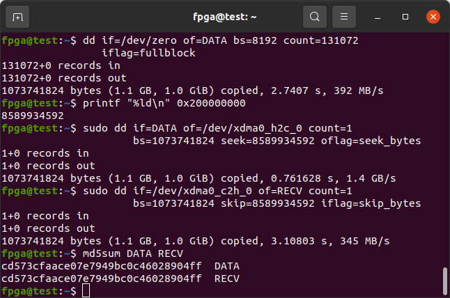
Test the first 1GB = 1073741824 bytes of the DDR4 memory space using a binary all-zeros file.
cd dma_ip_drivers/XDMA/linux-kernel/tools/
dd if=/dev/zero of=DATA bs=8192 count=131072
printf "%ld\n" 0x200000000
sudo dd if=DATA of=/dev/xdma0_h2c_0 count=1 bs=1073741824 seek=8589934592 oflag=seek_bytes
sudo dd if=/dev/xdma0_c2h_0 of=RECV count=1 bs=1073741824 skip=8589934592 iflag=skip_bytes
md5sum DATA RECV
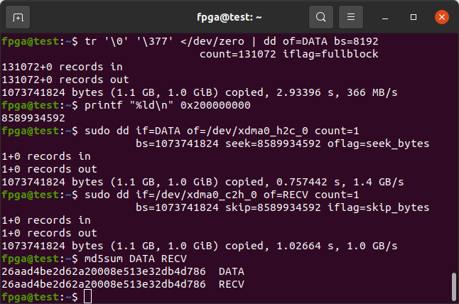
Test the first 1GB = 1073741824 bytes of the DDR4 memory space using a binary all-ones file.
cd dma_ip_drivers/XDMA/linux-kernel/tools/
tr '\0' '\377' </dev/zero | dd of=DATA bs=8192 count=131072 iflag=fullblock
printf "%ld\n" 0x200000000
sudo dd if=DATA of=/dev/xdma0_h2c_0 count=1 bs=1073741824 seek=8589934592 oflag=seek_bytes
sudo dd if=/dev/xdma0_c2h_0 of=RECV count=1 bs=1073741824 skip=8589934592 iflag=skip_bytes
md5sum DATA RECV
If you attempt to send data to the DDR4 address but get write file: Unknown error 512 it means DDR4 did not initialize properly or the AXI bus has encountered an error and stalled. Reboot and try again. If that fails, proceed to the Innova-2 DDR4 Troubleshooting project.
sudo ./dma_to_device --verbose --device /dev/xdma0_h2c_0 --address 0x0 --size 8192 -f TESTpread/pwrite combine lseek and read/write. Note the Linux Kernel has a write limit of 0x7FFFF000=2147479552 bytes per call.
#include <unistd.h>

ssize_t pread(int fd, void *buf, size_t count, off_t offset);
ssize_t pwrite(int fd, const void *buf, size_t count, off_t offset);
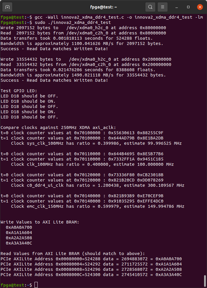
innova2_xdma_ddr4_test.c is a simple program that demonstrates XDMA communication in C using pread and pwrite to communicate with AXI Blocks.
gcc -Wall innova2_xdma_ddr4_test.c -o innova2_xdma_ddr4_test -lm
sudo ./innova2_xdma_ddr4_test
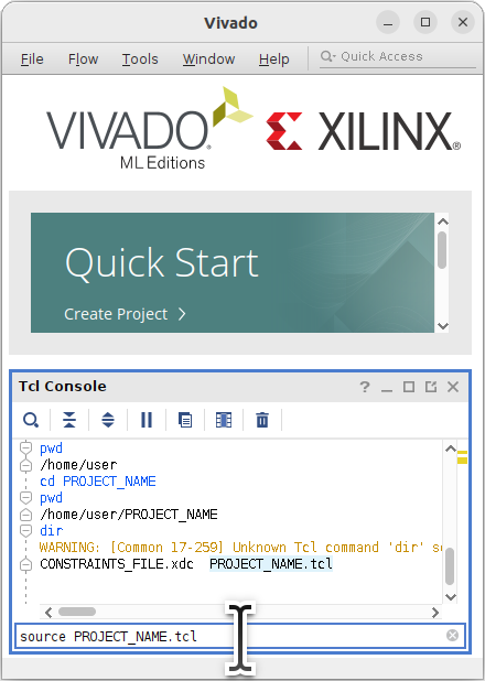
Run the source command from the main Vivado 2023.2 window.
cd innova2_4gb_adit_xdma_ddr4_demo
dir
source innova2_4gb_adit_xdma_ddr4_demo.tcl
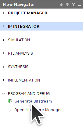
Click on Generate Bitstream.
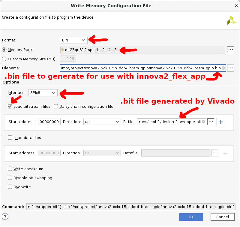
Once the Bitstream is generated, run Write Memory Configuration File, select bin, mt25qu512_x1_x2_x4_x8, SPIx8, Load bitstream files, and a location and name for the output binary files. The bitstream will end up in the innova2_4gb_adit_xdma_ddr4_demo/innova2_4gb_adit_xdma_ddr4_demo.runs/impl_1 directory as xdma_wrapper.bit. Vivado will add the _primary.bin and _secondary.bin extensions as the Innova-2 uses dual MT25QU512 FLASH ICs in x8 for high speed programming.
Proceed to Loading a User Image
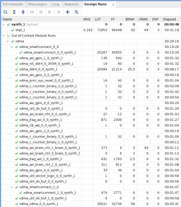
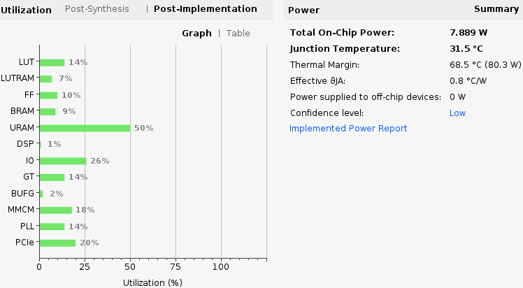
Design run details:
Resource Utilization Chart:
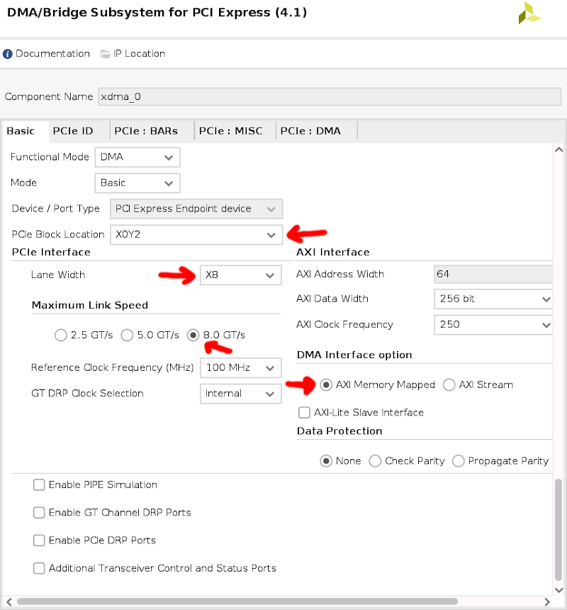
The Innova-2's XCKU15P is wired for x8 PCIe at PCIe Block Location: X0Y2. It is capable of 8.0 GT/s Link Speed.
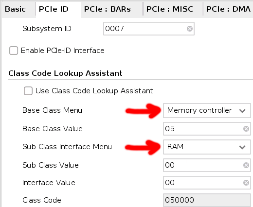
For this design I set the PCIe Base Class to Memory Controller and the Sub-Class to Other.
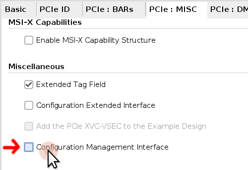
I disable the Configuration Management Interface.
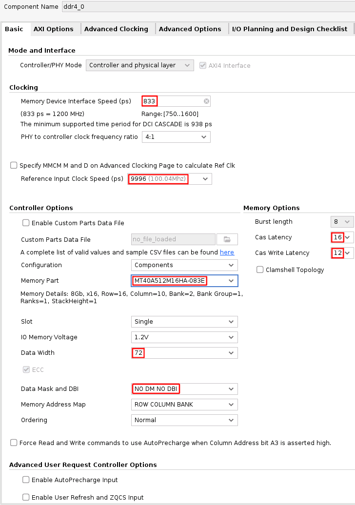
The DDR4 Memory Part is selected as MT40A512M16HA-083E which is compatible with the MT40A512M16JY-083E memory ICs with D9TBK FBGA Code on the 4GB Innova-2.
The DDR4 is configured for a Memory Speed of 833ps -> 1200MHz -> 2400 MT/s Transfer Rate. The DDR4 reference clock is 9996ps -> 100.04MHz. CAS Latency is set to 16 and CAS Write Latency is set to 12.
AGenchev has had success running the board at a 750ps -> 1333MHz -> 2666 MT/s Transfer Rate.
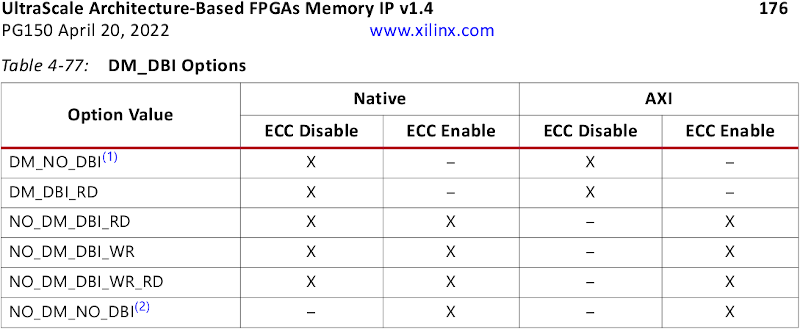
Data Mask and DBI is set to NO DM NO DBI which automatically enables ECC on a 72-Bit interface.
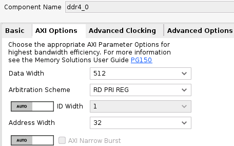
The Arbitration Scheme is set to RD PRI REG under AXI Options.
