PCBModelHelper is tool suite in order to help building Autodesk Fusion 360 3D model of PCB designed by Autodesk Eagle.
Eagle can manage 3D model for each device in component library and provides a function to export Fusion 360 3D model from board design.
This fucntion is useful to proceed collaborative work between electrical design and mechanical design.
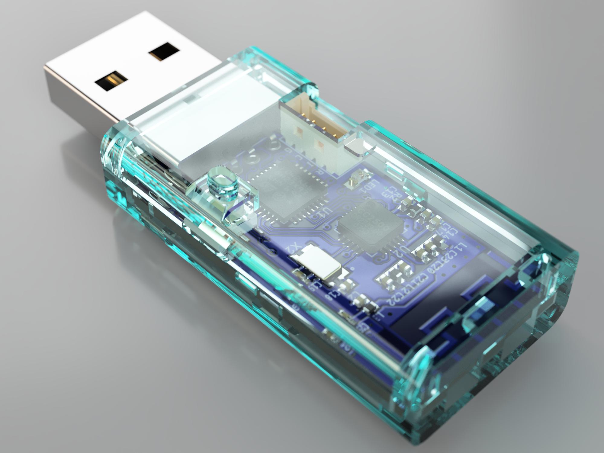
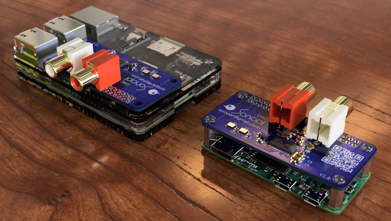
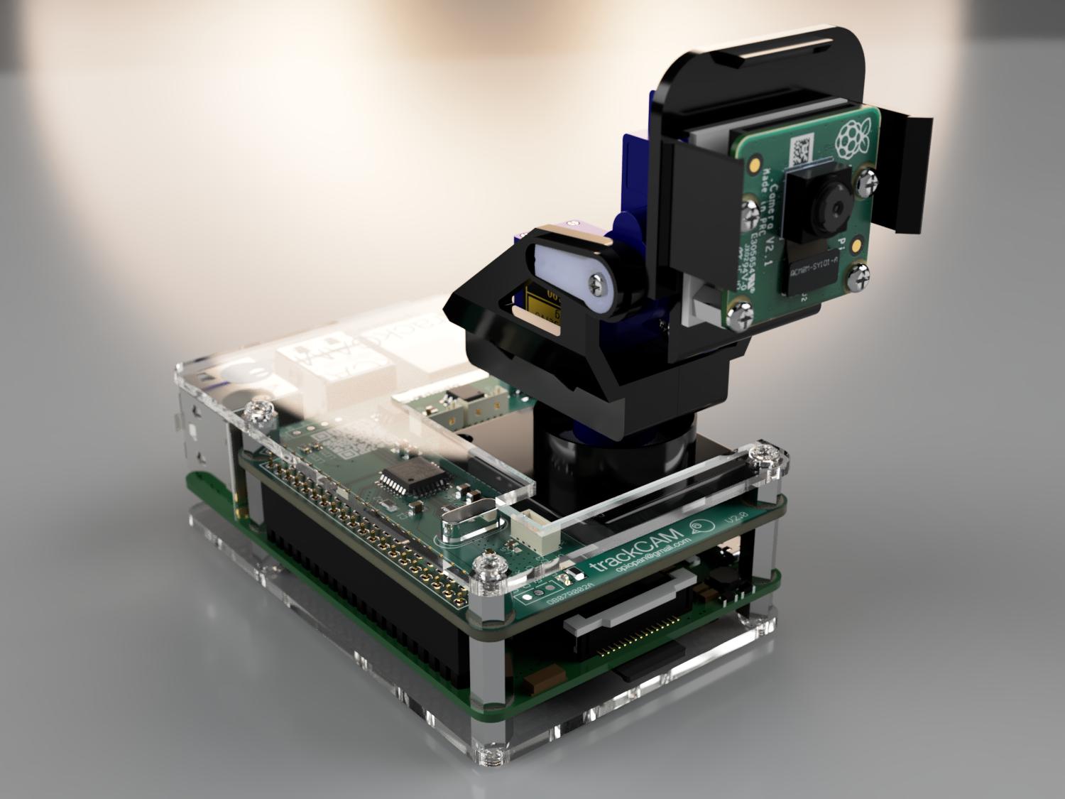
And Fusion 360 provides photo realistic 3D CG renderer also. This rendering quority is very high enough to use product catolog.
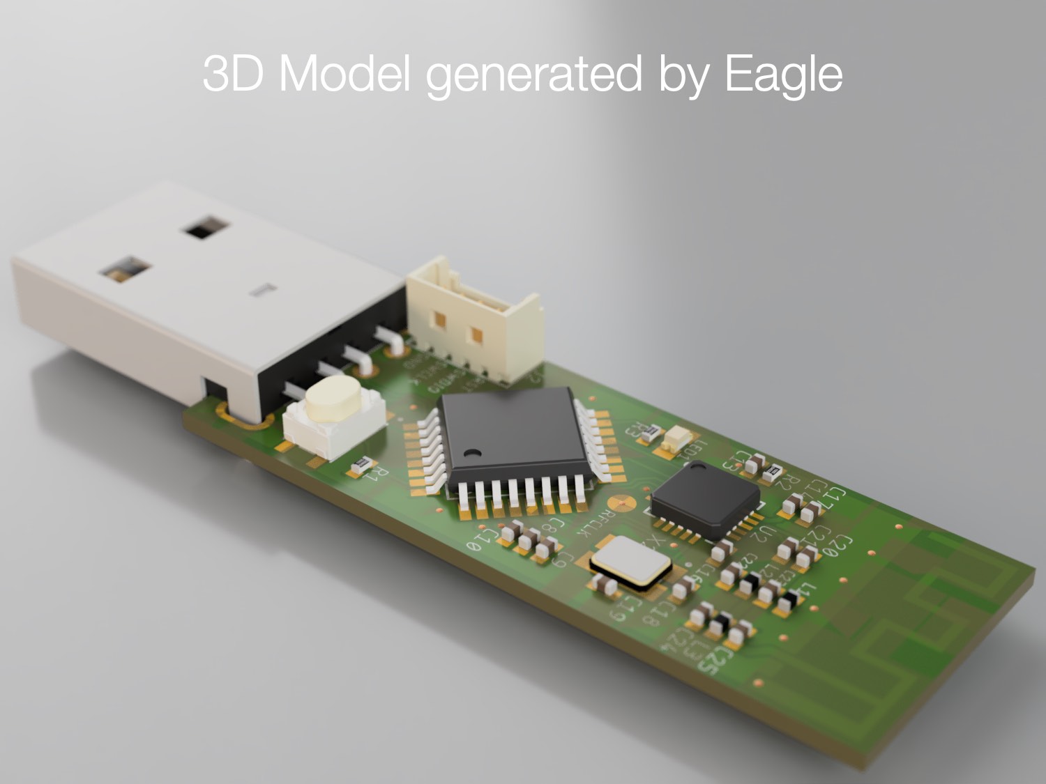
However, in case reding 3D model exported by Eagle, the result is quite dissappoointing finish as below example.
Since PCB board surface structure is expressed only one decal image, it's texture is flat and matte. We cannot feel metallic luster of pads or unevenness of circuit pattern from that image.
In addition, there are many artifact patterns on the board surface, I don't know the reason why.
And further more, all components on the board are also matt texture, because 3D model managed in Eagle library is imported as STEP formated data. Even if original 3D model made by Fusion 360 includes specific apearance metadata, such as albedo and/or heigt map, all metadata except color will be dropped when translating to STEP format.
As a result, rendered image looks like a clay work.
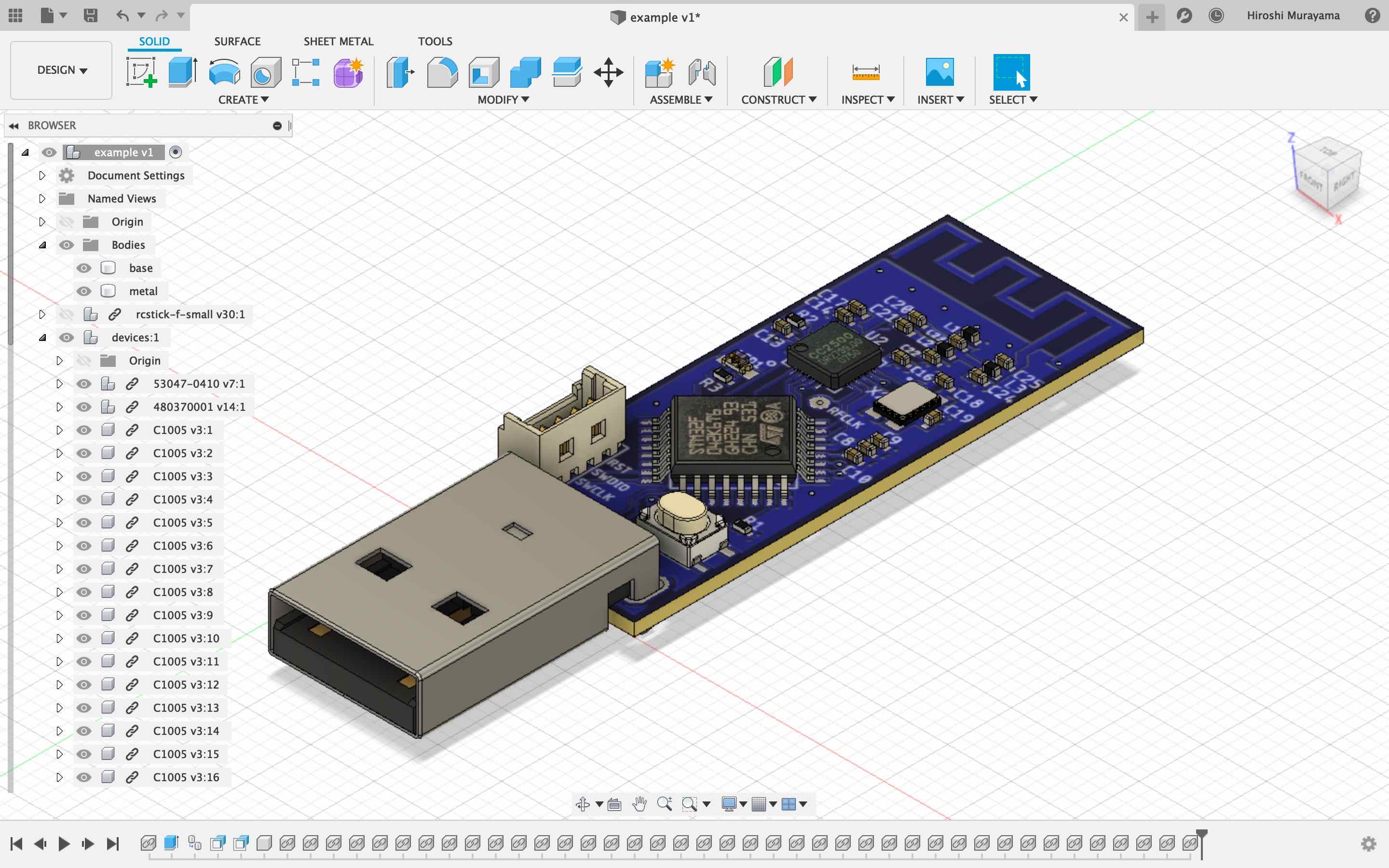
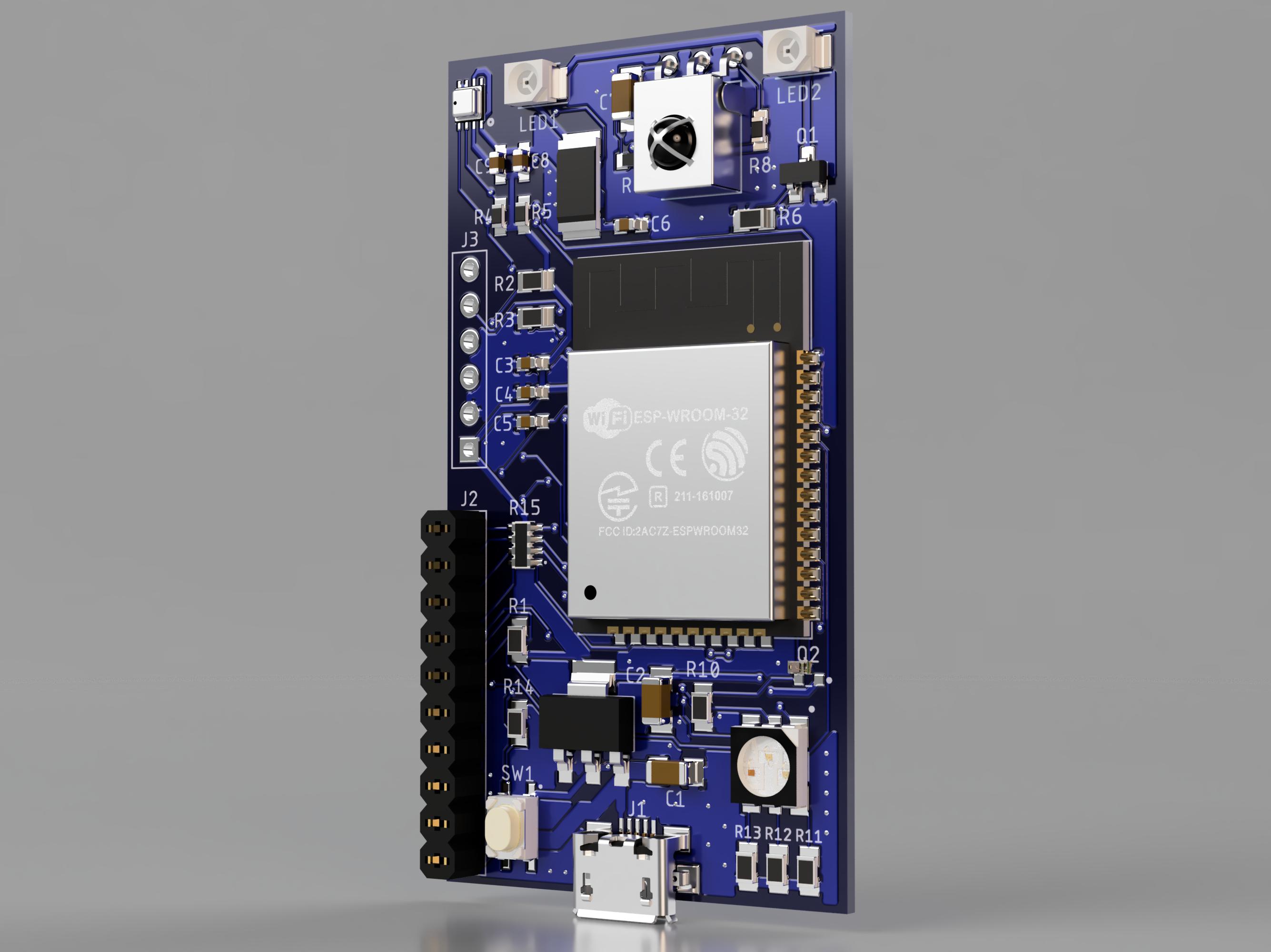
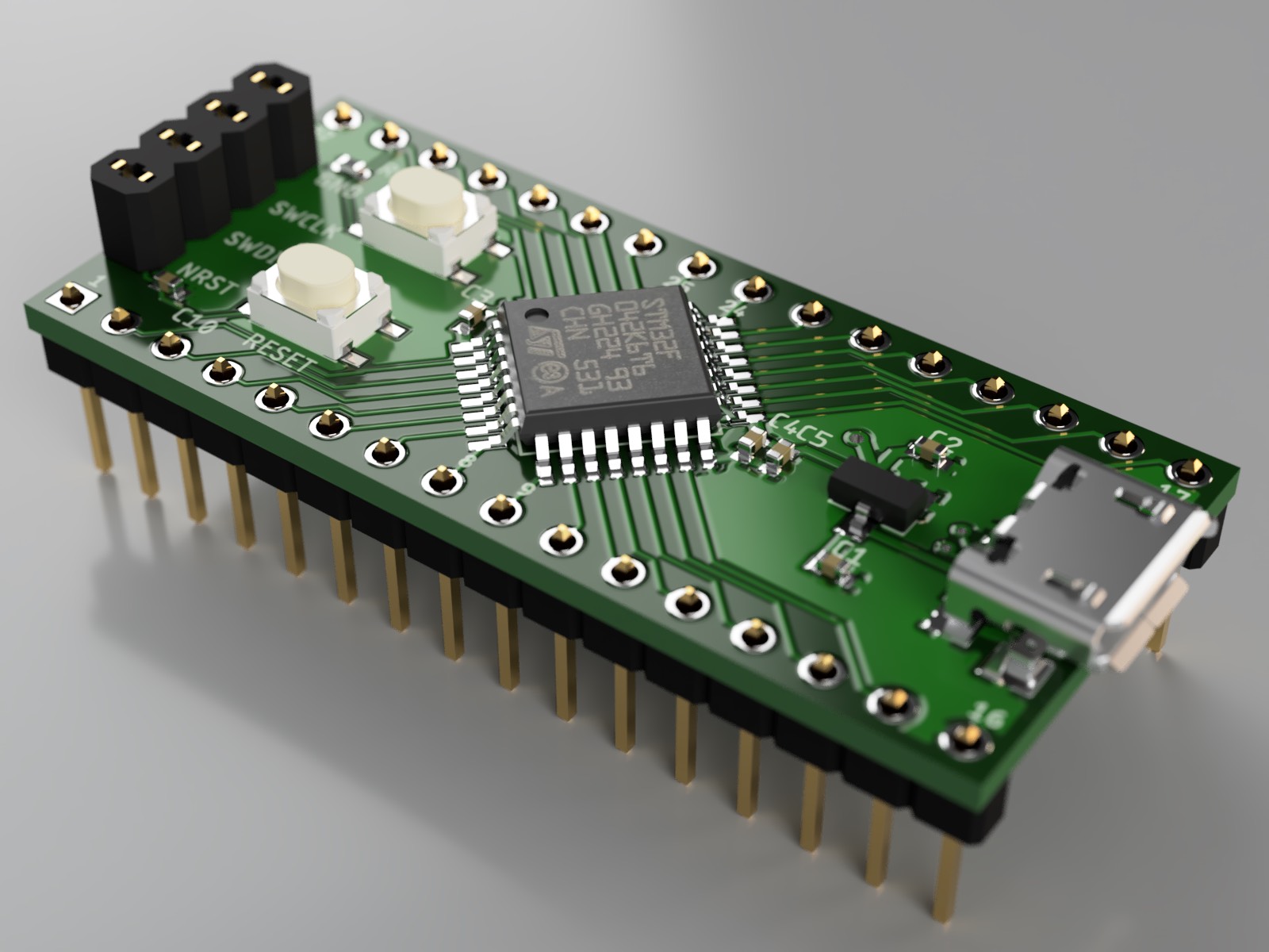
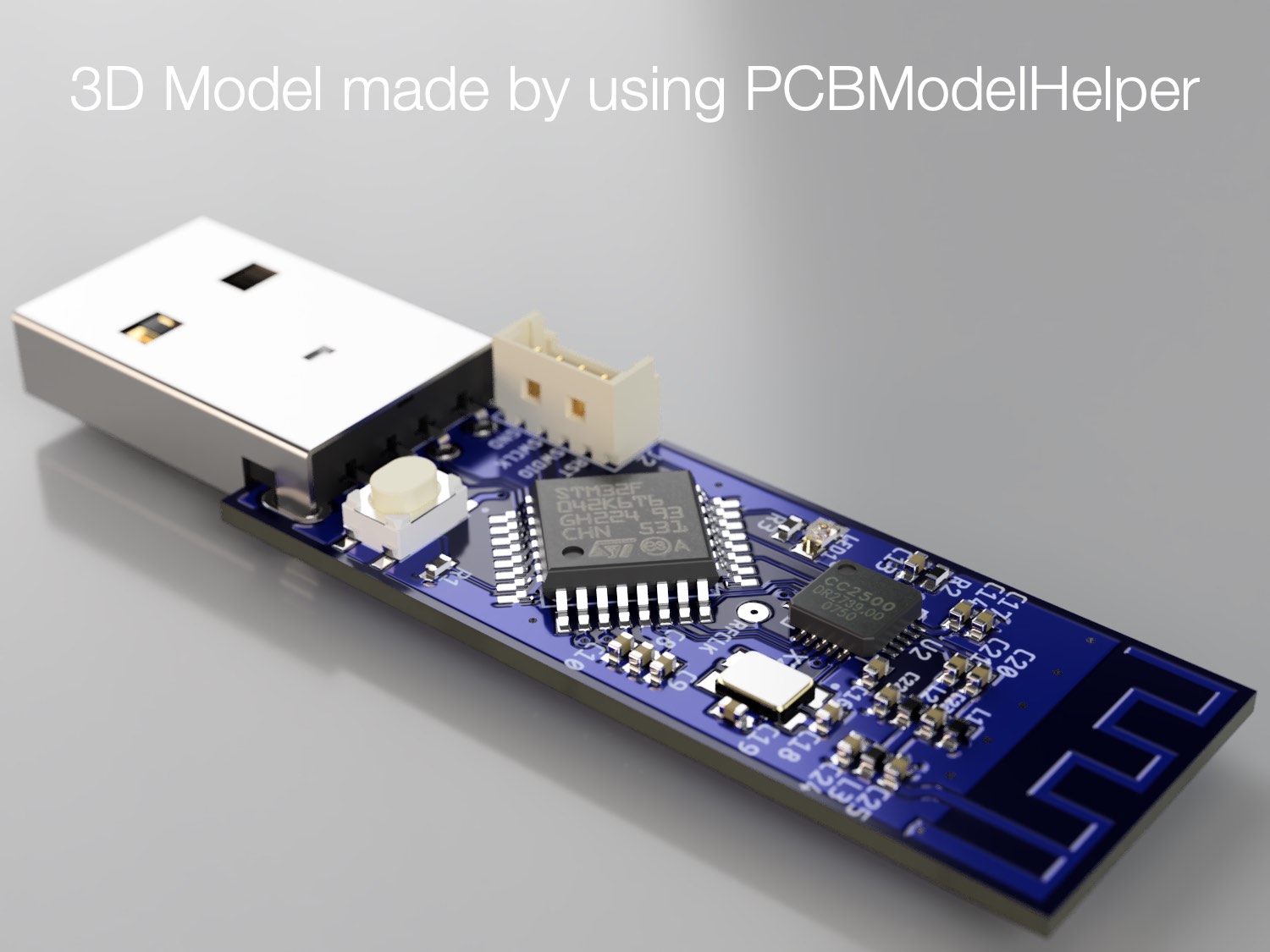
PCBModelHelper helps to make a 3D model which can be photo real rendered by Fusion 360. That model has a realistic appearance and original components 3d models that has complete appearance data are placed on the board.
Please compare between detail of following two examples after click to expand images
This tool suite include an Eagle ULP scripts and a Fusion 360 Add-on. Eagle ULP script can be run by just specify file path. On the other hand, Fusion 360 Add-on is need to register to Fusion 360 itself.
-
Clone this git repository
$ git clone https://github.com/opiopan/PCBModelHelper
-
Register Add-on program to Fusion 360
Enter to Fusion360 Design mode, then executeScripts and Add-inscommand inAdd-inspanel onTOOLStab.
Move to
Add-instab in theScript and Add-insDialog.
After that, push the plus button beside ofMy Add-inslabel.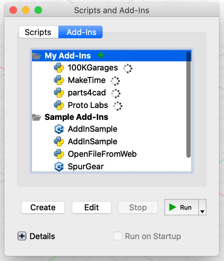
Folder selecting dialog is shown. Specify
fusion360-addinfolder under the root folder of git repository you cloned at step 1.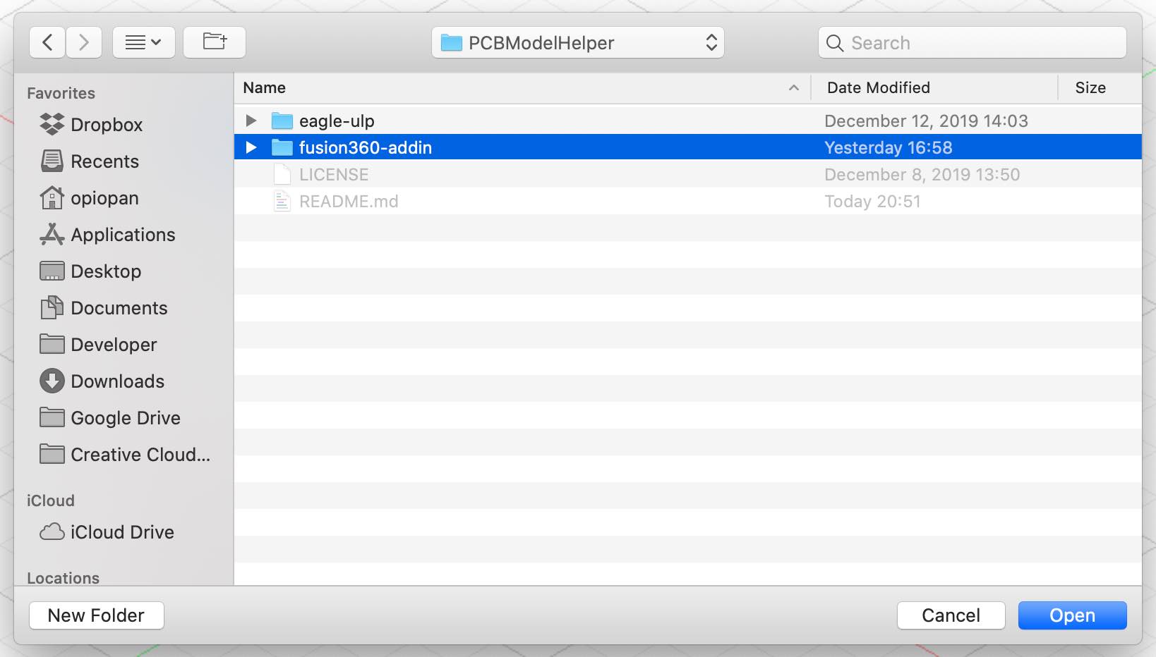
New add-in named
PCBModelHelperis added inMy Add-ins. Select this new add-in, then confirm thatRun on Startupis checked. After that, PressRunbutton.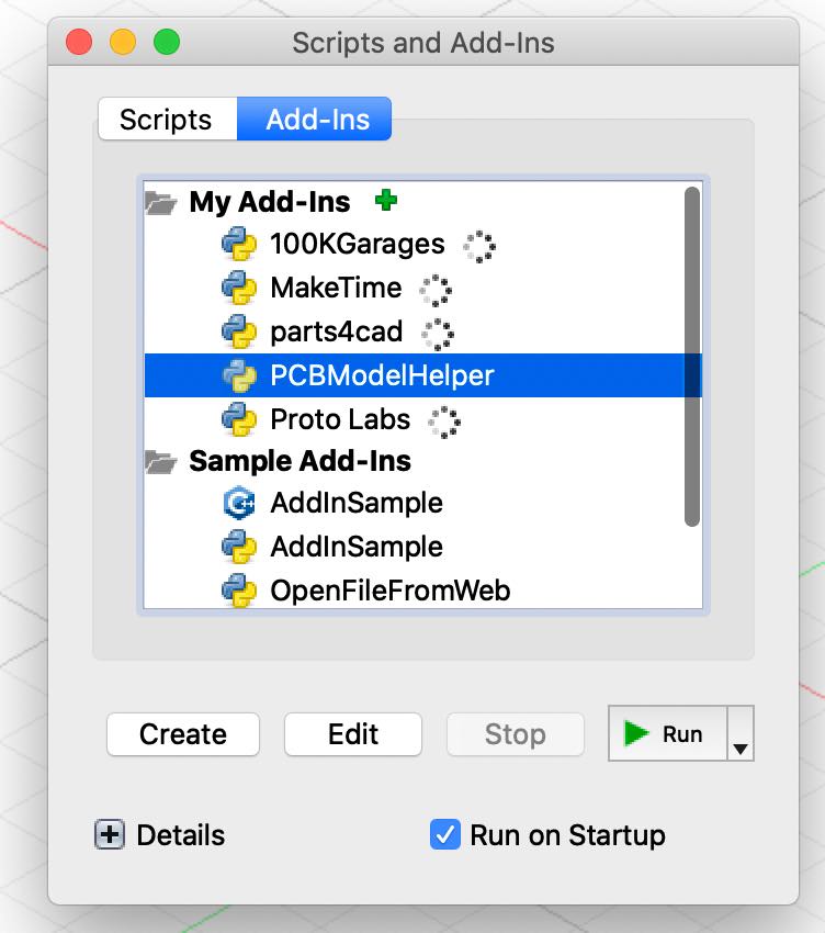
PCBModelHelper imports electric component models in order to place on PCB model. This add-in program requires that all component models are stored in same folder in the same project which PCB board model are stored.
Please place all 3D model refered from your bord design in same folder before start making PCB 3D model according to steps explaind below.
PCBModelHelper finds a component 3D model file corresponding to a eaach device used in your Eagle pcb design by using foot print name in Eagle library.
If names in Fusion repository is deferent from Eagle library, there is two way to inform correct name to PCBModelHelper.
One is editing a place-info file described later. Place-info file is a generated by Eagle ULP script included in PCBModelHelper, that contains location, rotation angle, and footprint name for each deves.
The other one is specifing correspondence between Eagle library footprint name and Fusion 360 model document name as Json dictionary data. If Json file named replace.json exists in directory fusion360-addin/Resources under directory that PCBModelHelper is cloned, PCBModelHelper replaces footprint name according to dictionary data.
Following file is a example of Json dictionary for footprint name replacement, dictionary key express footprint name in Eagle library and value exprress model document name of Fusion 360.
{
    "RCL_C0402_HS": "C1005",
    "MOLEX_48037-0001_1": "480370001",
    "RCL_L0402_HS": "L1005",
    "LED1608" : "led1608",
    "RCL_R0402_HS": "R0402",
    "SMT(4.2X3.2)": "SKRPACE010",
    "LQFP32-M": "LQFP32",
    "CC2500-RTY1_CC2500-HS": "CC2500RGPR",
    "CRYSTAL3225-HS": "CRYSTAL3225"
}Making PCB 3D model using PCBModelHelper is performed as following five steps.
- Exporting information to generate 3D model from Eagle
- Creating texture bitmaps for board appearance
- Generate board body
- Appling appearance to board body
- Placing device models on board
Tools provided by PCBModelHelkper is used at step 1, step 4 and step 5.
Step 2 is done by your favorite gerber file imaging tool.
Stope 4 is done by just pure human operation in Fusion 360, but it is not complex.
Export three kind of data as below from Eagle.
- Fusion 360 model data
- Gerber files
- Place-info file
Since Fusion 360 model and gerber files are generated by starndard function of Eagle, the explanation of detail steps are omitted in this document.
Place-info file is a generated by Eagle ULP script included in PCBModelHelper, that contains location, rotation angle, and footprint name for each deves.
On Eagle board design window, execute Run ULP command in File menu
Then, press Browse button at ULP dialog box in order to specify ULP script provided by PCBModelHelper.
ULP script to run is named export-placeinfo.ulp in dithrectory eagle-ulp under directory that PCBModelHelper is cloned.
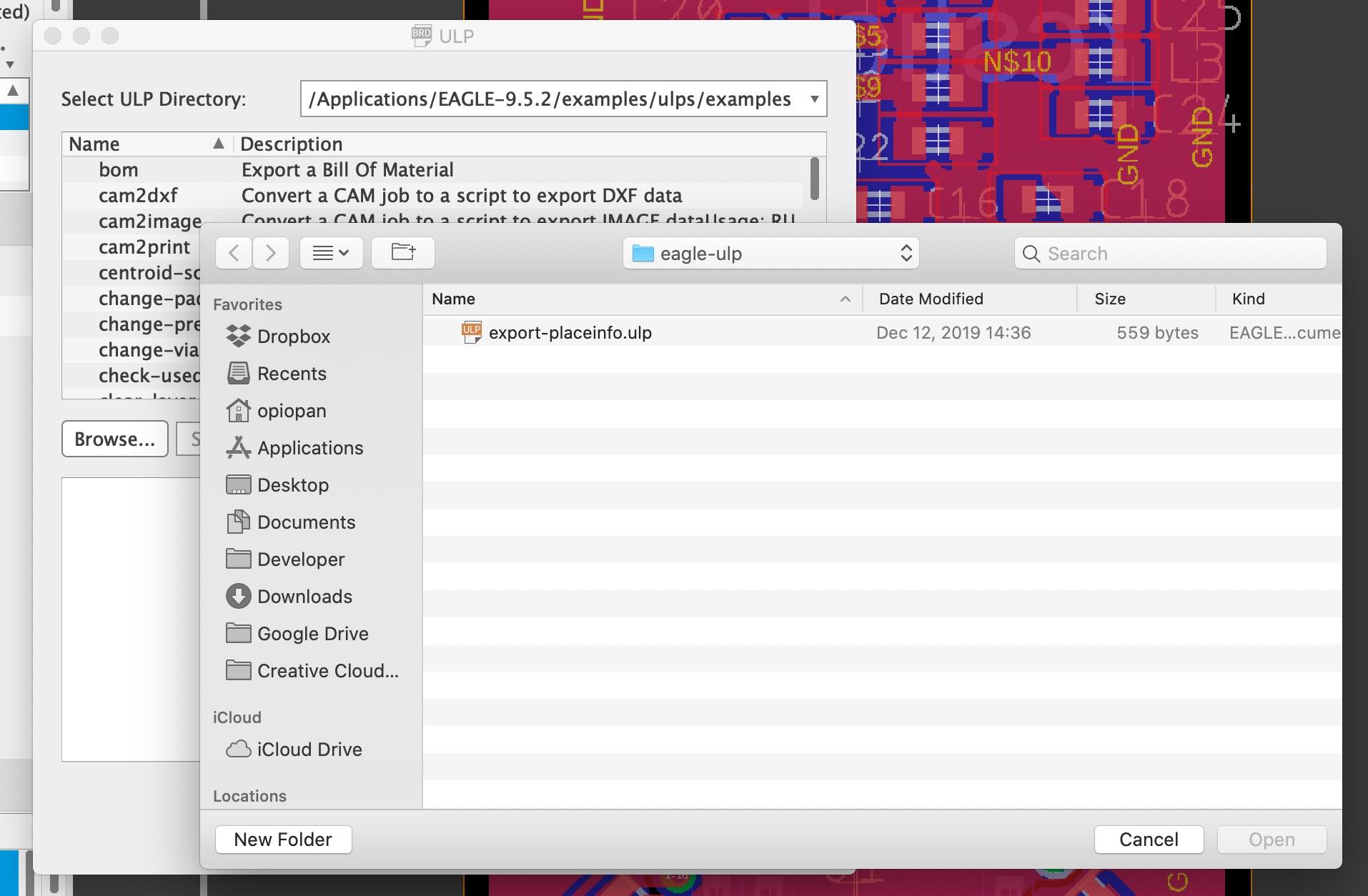
When export-placeinfo.ulp is executed, an dialog to specify file name and directory to save is shown. Specify place and file name that you want to save.
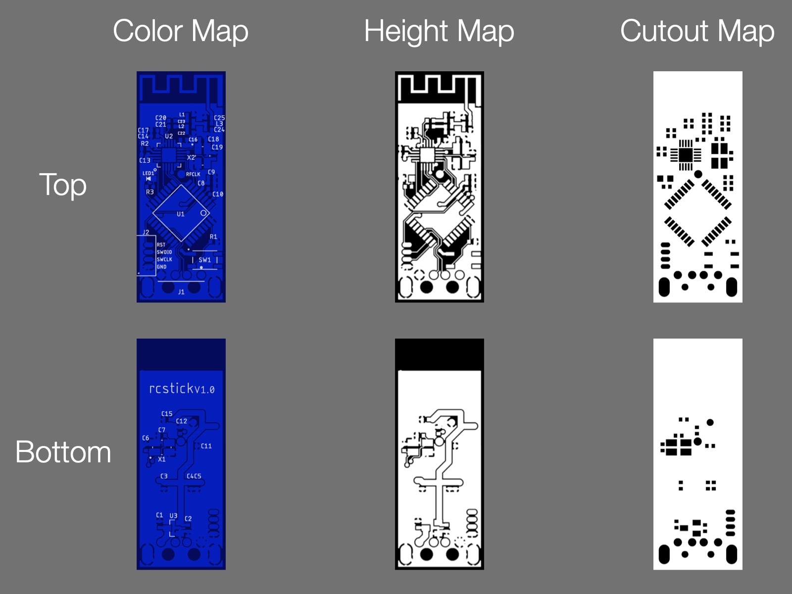
In this section, texture bitmaps using for board apearance.
Following three kind of bitmaps are used for both face, top and bottom. That means you must make six bitmaps.
-
Color map of reagion covered solder mask:
Created from gerber file of metal laryer and silk screen layer. -
Height map that express copper thickness:
Created from gerber file of metal layer.
In order to get better finish of rendering image, I recomend to blur this image a little bit. -
Cutout map that express region where solder mask does not cover:
Created from gerber file of solder mask layer.
Any tools which can imaging gerberfile may be suitable to generate these bitmaps.
I use pcb-tools for this step.
This python script is a example to generate these bitmaps using pcb-tools.
In my case, gerber file of each layer does not include bord profile (board outline) because I merge multiple gerberfiles to panelize. On the other hand, these texture bitmaps must made aligning with board outline.
Therefore, I translate original gerberfiles by this script in advance. This script uses pcb-tools-extension in order to merge original gerber file and outline layer.
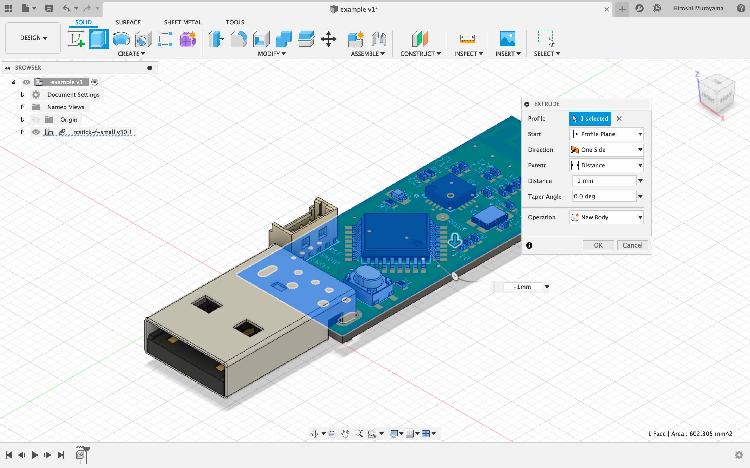
From this step, you use Fusion 360. At first, create new document and save with new name. Then, insert a PCB model generated by Eagle at step 1.
Select top face of board, then create a new body using Extrude command, and change name to base
Once new board body is created, original PCB model is not necessary. Hyde component of PCB model or delete that.
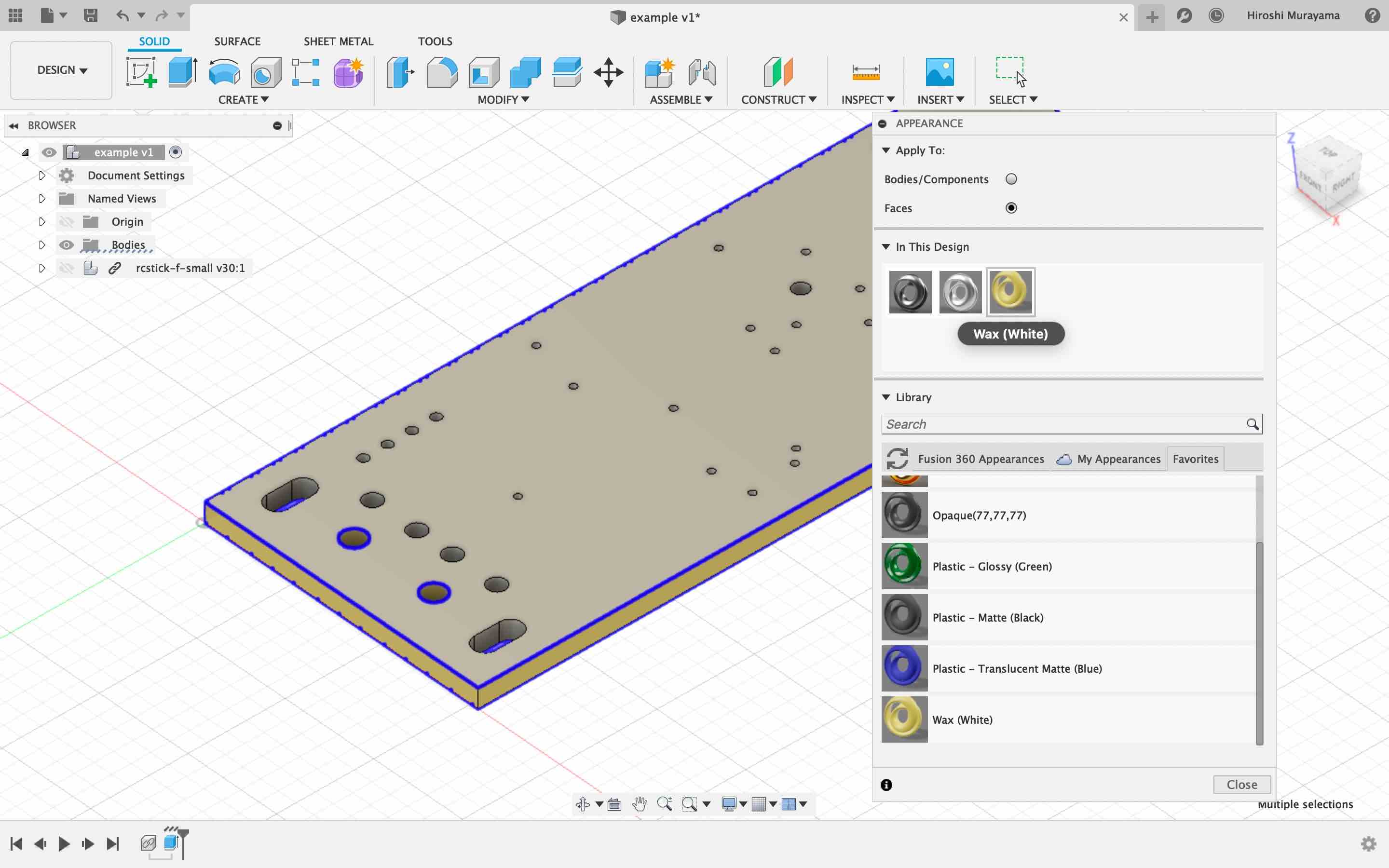
Next, Set base appearance to this body. This appearance is express via appearance. I usualy apply polished alminum appearance.
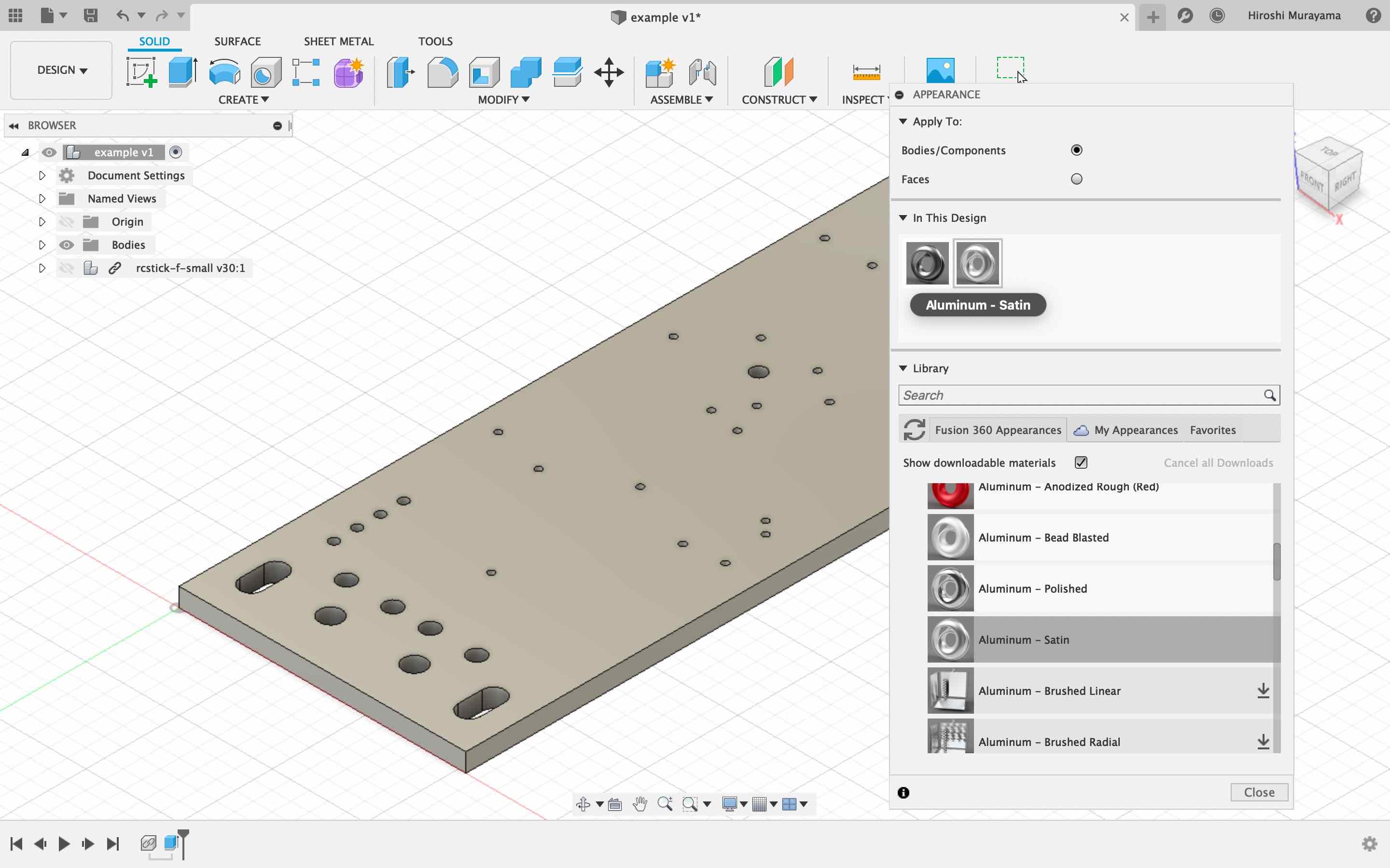
And so, Appearance for faces that PCB material is exposed is applied.
As PCB material, I use Wax appearance but color is changed to be yellowish.
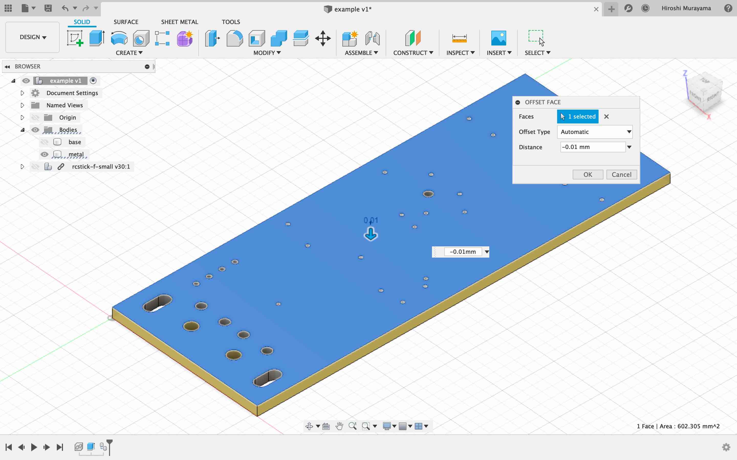
Copy body base and paste to same coordinate system. Then change name of new body to metal. This body represents metal pad on the boad.
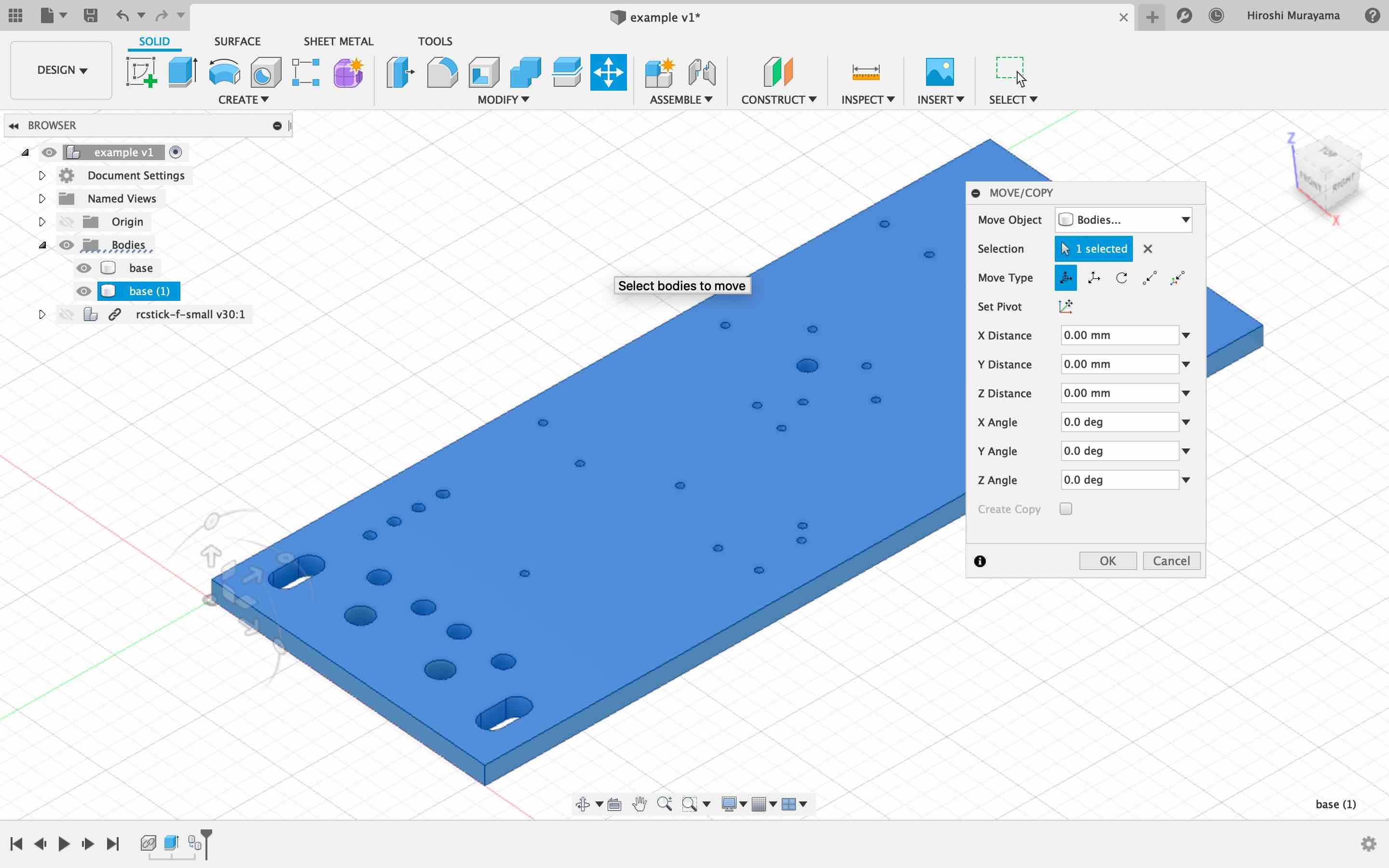
Offset both of top and bottom face of metal baody on the inside a little, I think 0.01mm is reasonable.
This operation is important to avoid some artifact in final rendering image.
Execute Generate PCB Appearances command in Modify panel.
As a result of execution, following dialog box is shown.
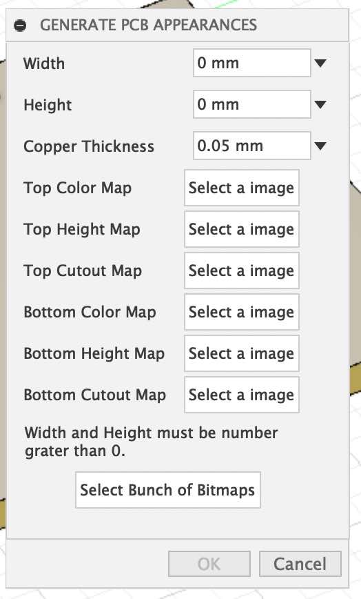
Input board width, board height, copper thickness, and sppecify all bitmaps created at step 2.
When you input board width, board height, and copper thickness, you can use Measure function that specify length by selecting a edge or two points.
If file name of bitmaps are according to following naming convention, you can specify a directory by press Select Bunch of Bitmaps button, instead of specifing each files.
| Bitmap Kind | File Name |
|---|---|
| color map for top face | pcb-top-base.png |
| height map for top face | pcb-top-hmap.png |
| cut map for top face | pcb-top-mask.png |
| color map for bottom face | pcb-bottom-base.png |
| height map for bottom face | pcb-bottom-hmap.png |
| curt map for bottom face | pcb-bottom-mask.png |
Once all information are filled, press OK button in order to generate appearances.
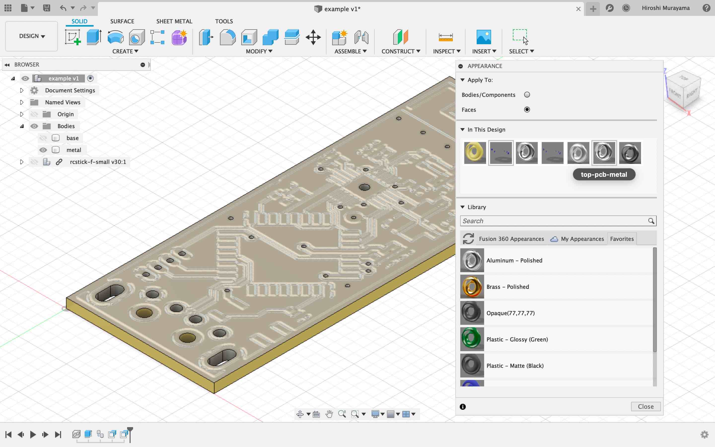
Then, execute Appearances command in Modify panel, and confirm following four appearances are added in your design.
- top-pcb-base
- bottom-pcb-base
- top-pcb-metal
- bottom-pcb-metal
Change body visibility that base is visible and metal is hidden, then apply top-pcb-base appearance to top face and bottom-pcb-base appearance to bottom face.
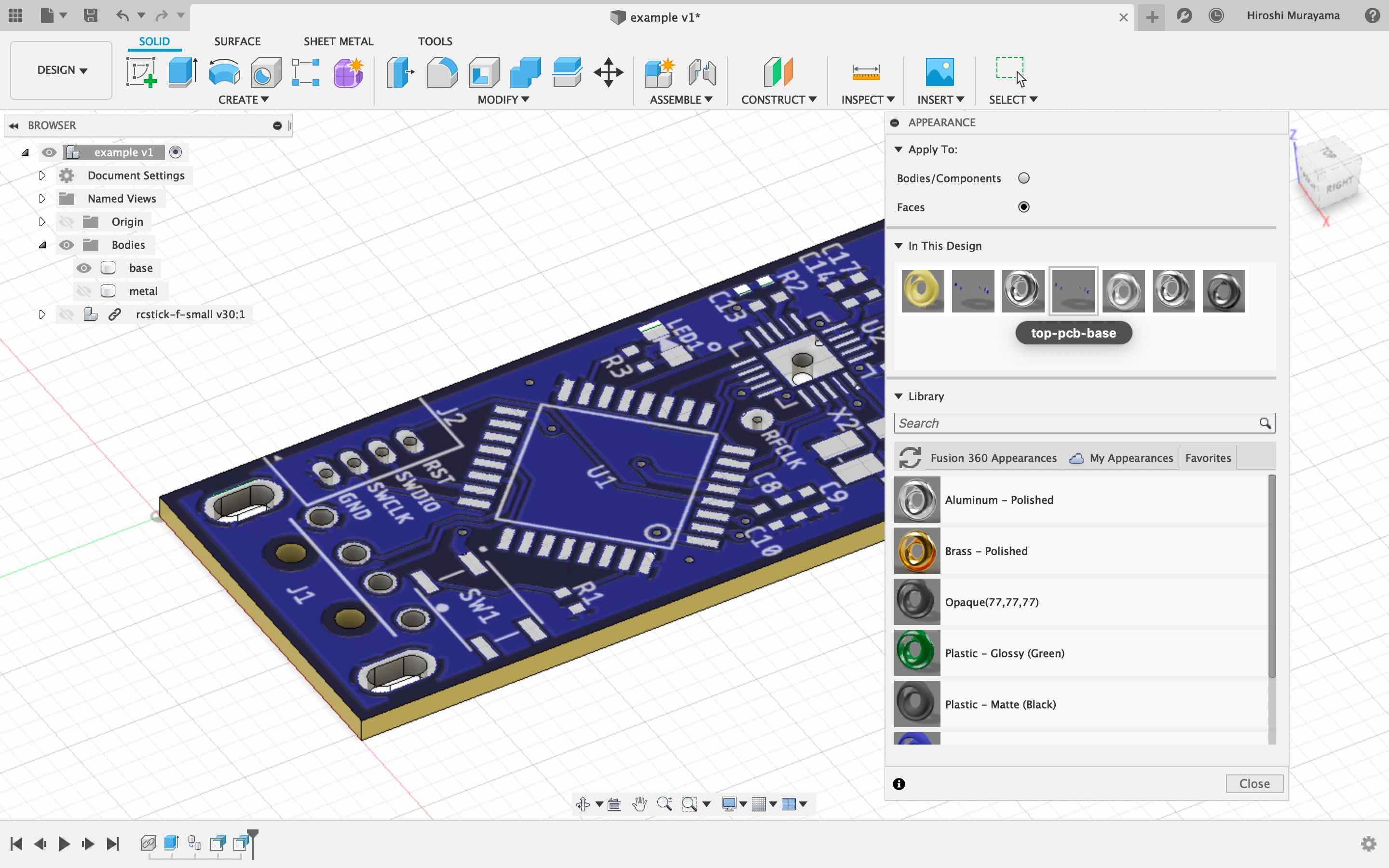
metal body's appearance is also arranged.
Change body visibility that base is hidden and metal is visible, then apply top-pcb-metal appearance to top face and bottom-pcb-metal appearance to bottom face.
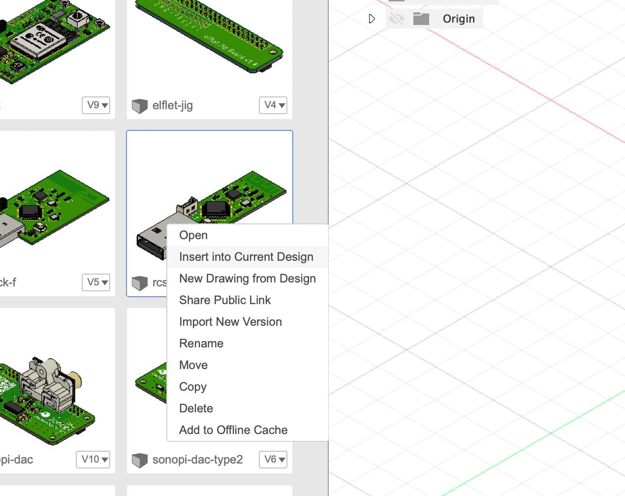
Before proceed this last step, confirm that your device model repository is included in current project.
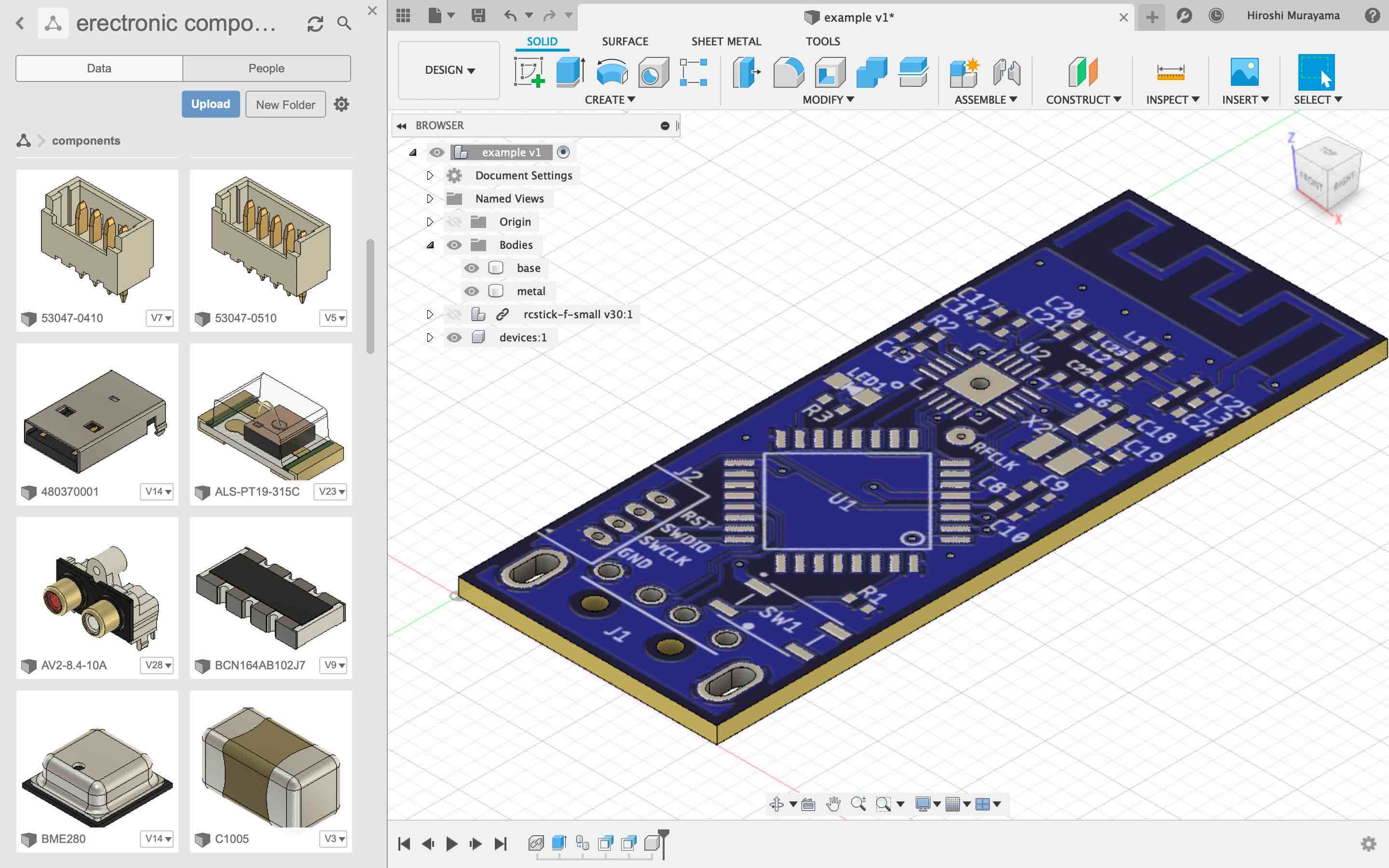
Select a component to insert device models. Of cause root component can be specified.
Then, execute Place components on PCB command in Insert panel.
As a result of execution, following dialog box is shown.
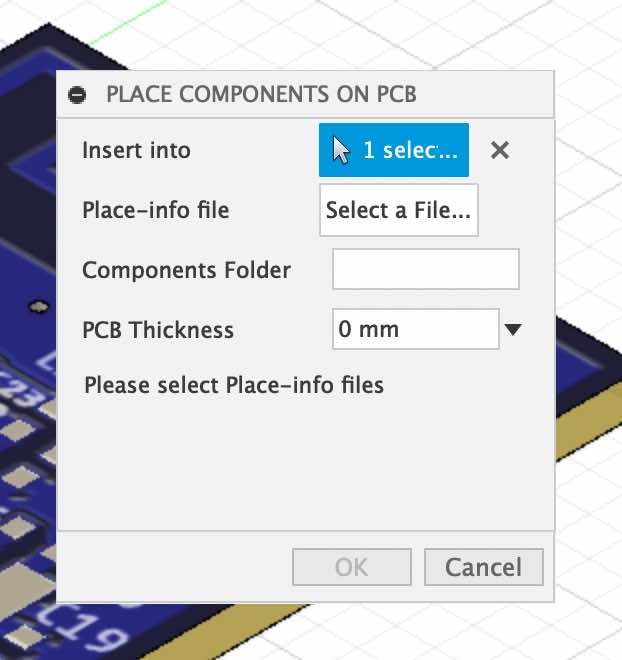
Specify place-info file exported at step 1, your device model library folder path in current project, and board thickness. then press OK button.
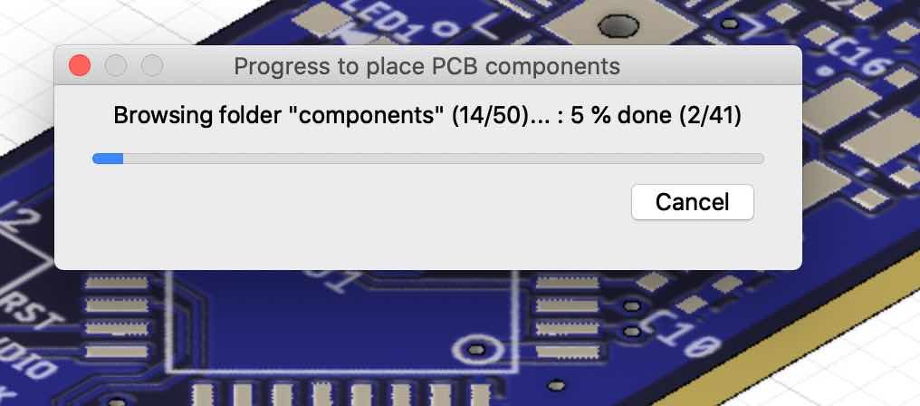
Progress dialog is shown, and it may take a couple of minutes.
Finaly, It's complete to make PCB 3D model for rendering.