This is a solution for the assignment for NI-DS scratch detection link
The goal is to use the training data to build a model that can predict, given a certain wafer map, to predict whether a given die belongs to scratch or not.
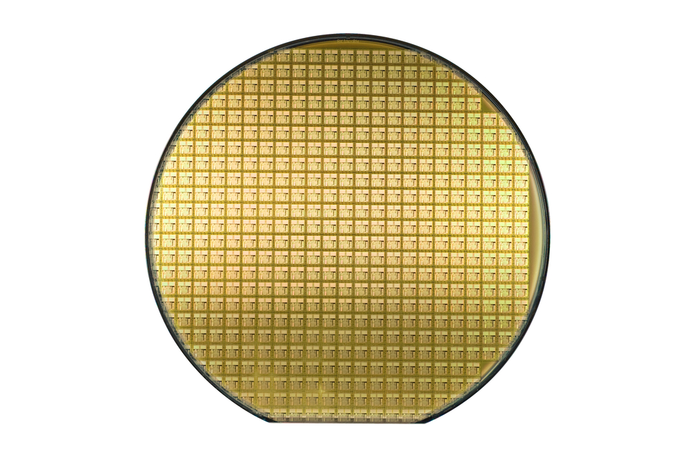
In the semiconductor industry, "wafers" are thin discs of semiconductor material, such as silicon, used to fabricate microelectronic devices such as transistors, integrated circuits, and other components. A single wafer can contain hundreds or thousands of individual devices, known as "dies", which are typically cut or "diced" from the wafer after the manufacturing process is completed.
You can read more about semiconductor here: Introduction to Semiconductors
Fig.1 - An example of a standard waferOne of the challenges in manufacturing wafers is to identify and isolate defects, including scratches, which can affect the performance and reliability of the resulting devices.
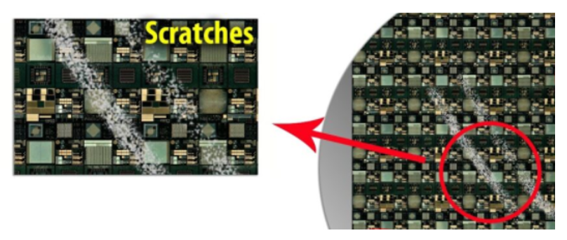
Scratches are seen as elongated clusters of bad dies that have a high aspect ratio, meaning they are relatively thin and long compared to their width. They can be caused by equipment misalignment or mishandling by humans, and may contain latent defects that can affect the performance of the devices. Scratches may not always be continuous, so sometimes there may be good dies within the scratch. These good dies are often marked for removal in a manual process called "Inked dies"
Fig.2 - A scratch on a wafer - an optical viewIn the data that you receive, there may be faulty dies that are part of a scratch, which are labeled as "Scratch" as well as a few good dies that are part of a scratch, which are labeled as "Ink."
Many times, the Scratch Detection process will be done on the logical wafer map and not on a visual image of it.
The data that you received is called "wafer map" as it maps the status of all dies in the wafer.
The dies in the wafers are tested in a large number of stations, operations, and in each operation it is possible to create a map of the dies in this operation by coloring the good dies in a certain color and the faulty dies in another color.
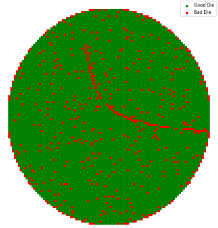
Fig.3 - A logical wafer map in a certain operation. good dies in green and bad dies in redDid you notice a scratch on this wafer?
Well, with our eyes it is easy to notice the scratch that comes out from the right side in the center of the wafer.
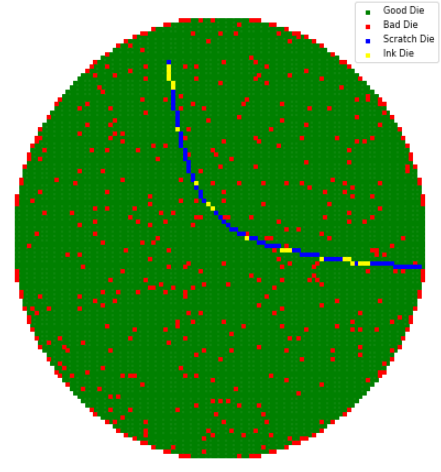
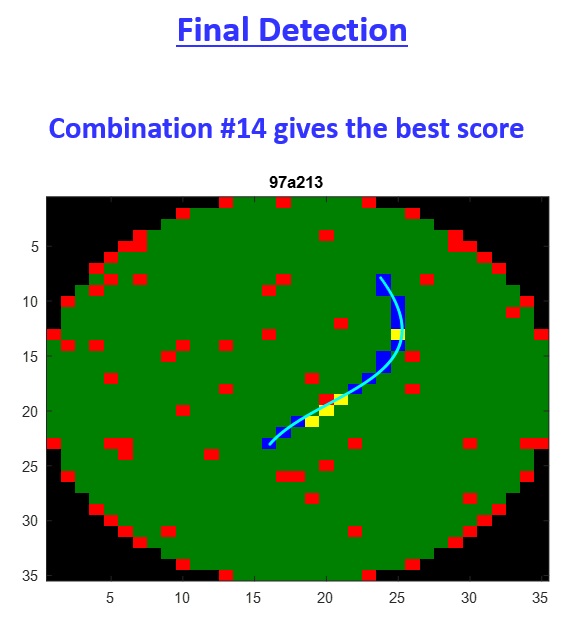
Note, that this scratch is not continuous, meaning, not all the dies which are placed on this scratch are considered faults in this operation. We have to identify all scracthed dies including bad & good. The good dies that are part of the scartch have to be itendified actively in order to be killed. This process is called "inking".
We kill them because we fear that a physical scratch on the silicon wafer is what caused the sequence of these faulty dies, therefore even dies that passed the tests may be of low quality because they were damaged by the scratch on which they are placed.
Fig.4 - A wafer map in a certain operation with scratch detection marks. good dies in grenn, bad dies in red, scratch in blue, ink in yellow