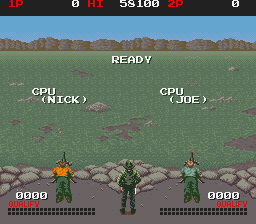
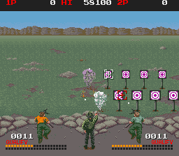
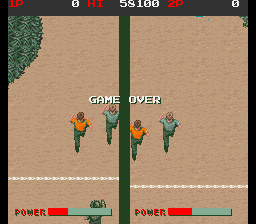
Konami developed a graphic chip called 007121. This was used in several games. This project aims to accurately replicate those games in modern electronics, namely FPGA systems.
| Name | JT Core | Main CPU | Sound CPU | K007121 units | Audio |
|---|---|---|---|---|---|
| Contra | contra | HD63C09EP | 68B09EP | x2 | YM2151 |
| Combat School | comsc | 6309 | Z80 | x2 | YM2203 + UPD7759 |
| Haunted Castle | KONAMI | Z80 | x2 | YM3812 + K051649 | |
| Fast Lane | 6309 | - | x2 + K051733 | K007232 x 2 | |
| MX5000 | 6309 | Z80 | x1 | YM2151 + K007232 | |
| Labyrinth Runner | 6309 | - | x1 + K051733 | YM2203 x 2 |
Binary RBF files for MiST, MiSTer and SiDi will be provided for in https://github.com/jotego/jtbin
You need to have Quartus installed in a linux machine. Clone this repository and
its submodules following standard git instructions. Go to the root folder and
type source setprj.sh. Now you can compile the core with jtcore contra -mist
Use -mister or -sidi if appropriate.
Use the mra file in rom/mra for MiSTer. For MiST/SiDi, convert the mra to a rom file using the mra tool.
| Name | Purpose | Author | URL |
|---|---|---|---|
| JT51 | YM2151 sound | jotego | https://github.com/jotego/jt51 |
| JTFRAME | FPGA framework | jotego | https://github.com/jotego/jtframe |
Furrtek made a full RE of this chip here
The internal register mapping has R/W access from the CPU. If the row scroll registers are prevented from reading, Combat School boots up with an error on "zure RAM", note that "zure" is Japanese for scroll.
| Address | Purpose |
|---|---|
| 20-3F | zure RAM - row scroll |
| 40-5F | text tilemap selection (over scroll tilemap) |
| 2000-2FFF | VRAM |
| 3000-3FFF | OBJ RAM |
Attribute byte
| Bits | Usage | Condition |
|---|---|---|
| 2:0 | Palette | |
| 3 | Palette MSB | MMR[6][0] high |
| 6:3 | Bank bits 4:1 | Enabled by MMR[4] and MMR[5] |
| 7 | Bank bit 0 |
| Pin Name | Number | I/O | Usage |
|---|---|---|---|
| H2 | 68 | O | 0=output ROM addr is for tilemaps, 1=objects |
| A13 | 109 | I | 0=internal config registers, 1=VRAM |
| A12 | 52 | I | 0=tilemaps, 1=objects |
| NXCS | 63 | I | chip select |
| COA6 | 81 | O | palette RAM address 6 |
| COA5 | 20 | O | palette RAM address 5 |
| COA4 | 80 | O | palette RAM address 4 |
| COA3 | 79 | O | palette RAM address 3 |
| COA2 | 18 | O | palette RAM address 2 |
| COA1 | 16 | O | palette RAM address 1 |
| COA0 | 17 | O | palette RAM address 0 |
| CK24 | 1 | I | 24MHz input clock |
| CK2 | 4 | O | CK24/4 (6MHz output clock) |
| NE | 65 | O | E signal for M6809 |
| NQ | 66 | O | Q signal for M6809 |
There are 8 programmable registers, most of them are 8-bit long, some have unused bits which do not connect to any physical register. Register cannot be read back.
Blank cells refer to 0/0.
The jotego nickname had already been used by other people so on some networks you will find me as topapate.
Contact via:
You can show your appreciation through
- Patreon: https://patreon.com/topapate
- Paypal: https://paypal.me/topapate
