This is a project report submitted by Vardhan Suroshi to Prof. Mahesh Awati, Department of Electronics and Communication Engineering PES UNIVERSITY in the 6th semester for the course "Memory Design and Testing" (Course Code: UE20EC343) during the academic year 2022-23 The project involves the design of a 4X4 SRAM Memory Array using Cadence Virtuoso built using GPDK 180nm
Project guide: Prof. Mahesh Awati, Department of Electronics and Communication Engineering, PES UNIVERSITY, Electronic City, Bangalore-560100, Jan-March 2023
- Design of 4X4 SRAM Memory Array Using Cadence Virtuoso
- Implementation and Simulation Results
- 6T SRAM Cell
- 4x4 Memory Array
- Conclusion
- Acknowledgment
In modern computer systems, various types of memory are employed to store and manage data. These memories can be broadly categorized into the following category
Volatile memory is temporary storage that loses its contents when the power is turned off. The primary volatile memory types include RAM. RAM is a fast, volatile memory used for temporary data storage. It allows quick read-and-write access, making it essential for active applications and the operating system. There are mainly two kinds of RAM:
-
Dynamic Random Access Memory (DRAM): DRAM is a type of RAM that stores each bit of data in a separate capacitor within an integrated circuit. It requires periodic refresh cycles to maintain data integrity.
-
Static Random Access Memory (SRAM): SRAM is another form of volatile memory that does not require refreshing. It is often used for cache memory in CPUs due to its faster access times compared to DRAM.
Non-volatile memory retains its data even when power is turned off. Common types of non-volatile memory include:
-
Read-Only Memory (ROM): ROM is used to store permanent data, typically in firmware and software. It is non-volatile and is not easily modified.
-
Flash Memory: Flash memory is a type of non-volatile storage that can be electrically erased and reprogrammed. It is commonly used in USB drives, SSDs, and memory cards.
SRAM is a type of volatile memory that uses bistable latching circuitry to store each bit. Unlike DRAM, SRAM does not require refreshing, making it faster and more energy-efficient. SRAM cells offer an advantage over other types of volatile memory, such as Dynamic Random Access Memory (DRAM), which is slower and requires periodic refresh cycles. This makes SRAM cells a fundamental building block of modern computing systems and a key technology for achieving high-speed data processing.
SRAM is widely used in various applications due to its speed, low power consumption, and suitability for cache memory. Some key applications include:
-
Cache Memory: SRAM is commonly used as cache memory in CPUs to provide fast access to frequently used data.
-
Register Files: SRAM is used in register files within microprocessors for storing temporary data during computation.
-
Networking Devices: SRAM is employed in networking devices for buffering and storing routing tables.
-
Embedded Systems: SRAM finds applications in embedded systems, providing quick access to critical data.
The primary objective of this project is to gain a comprehensive understanding of Static Random Access Memory (SRAM) by designing a complete 6T SRAM cell, including its peripheral circuitry, using Cadence tools on the 180nm technology node (GPDK180). The project aims to explore various aspects of SRAM design with a focus on optimizing read and write stability, transistor sizing for enhanced data stability, and the design of peripheral circuits to achieve faster read and write operations
The project aims not only to achieve the defined objectives but also to foster a collaborative environment for knowledge sharing and continuous improvements. Feel free to explore the repository, contribute, raise issues, and engage in discussions as we work together to achieve the project goals.
The SRAM memory architecture employs a systematic arrangement of cells, word lines, and bit lines, all orchestrated through precise address decoding. The design facilitates efficient read and write operations, crucial for the reliable functioning of SRAM in various computing applications.
- The SRAM memory architecture is structured around the fundamental unit known as the SRAM cell. This cell, typically a 6T configuration, holds a bit of data, representing either a 1 or 0. The architecture is designed for efficient data storage and retrieval, with specific components contributing to its functionality.
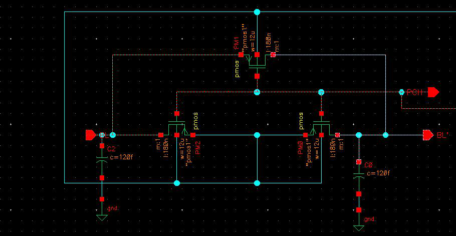
- Pre-circuit is used to pre-charge the bit lines to Vdd before the Read
operation. It consists of:
-
Equalizer transistor which reduces the required pre-charge time by ensuring that both bit lines are at nearly equal voltages even if they are not pre-charged to Vdd.
-
Bias transistors that pull each of the bit lines to Vdd.
-
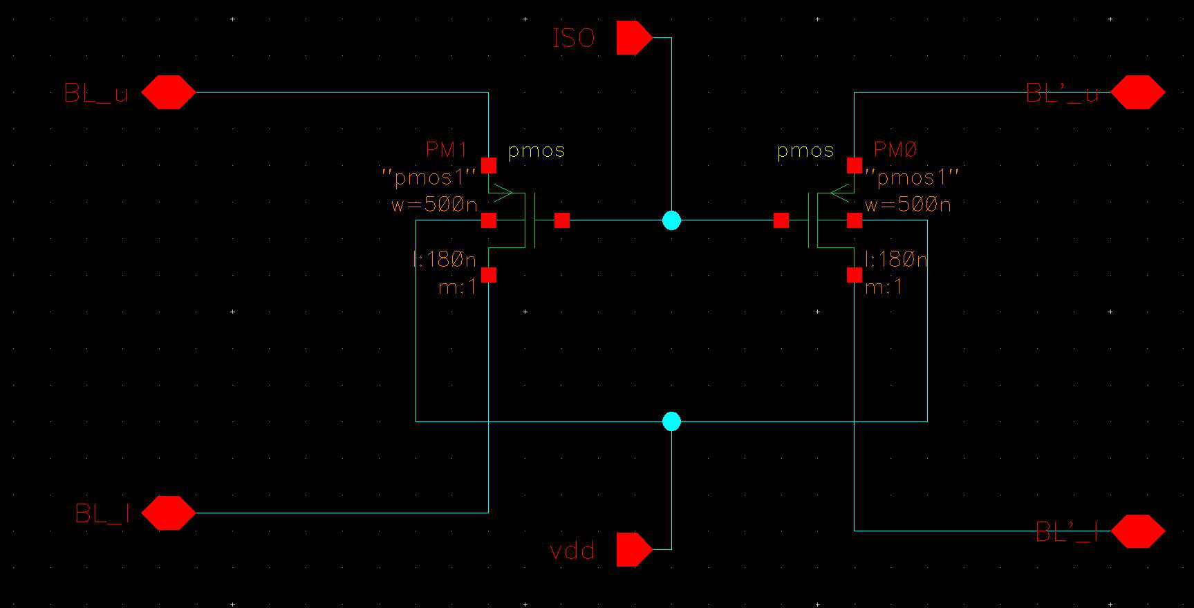
- An isolation circuit is used to isolate the sense amplifier from the bit lines once a small change on the bit lines is detected.
- The sense amplifier is responsible for detecting the value stored in the SRAM cell during the read operation and displaying that value at the output.
- The read circuitry includes a sense amplifier, a crucial component that amplifies the small voltage swing on bit lines to recognizable logic levels. This amplification is essential for reliable data interpretation during read operations.
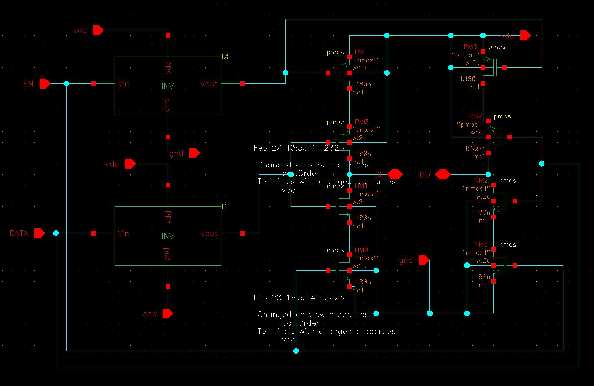
- The write driver circuit is responsible for writing the data onto the bit lines BL and BL' during the write operation
- Write driver circuits play a vital role in the writing process. They force one of the bit-lines to zero while maintaining the pre-charged value on the other bit-line. This controlled manipulation ensures accurate data storage within the SRAM cell.
- The row and column (or groups of columns) to be selected within the storage array are determined through the decoding of binary address information. This addressing mechanism ensures precise access to the desired data within the SRAM architecture.
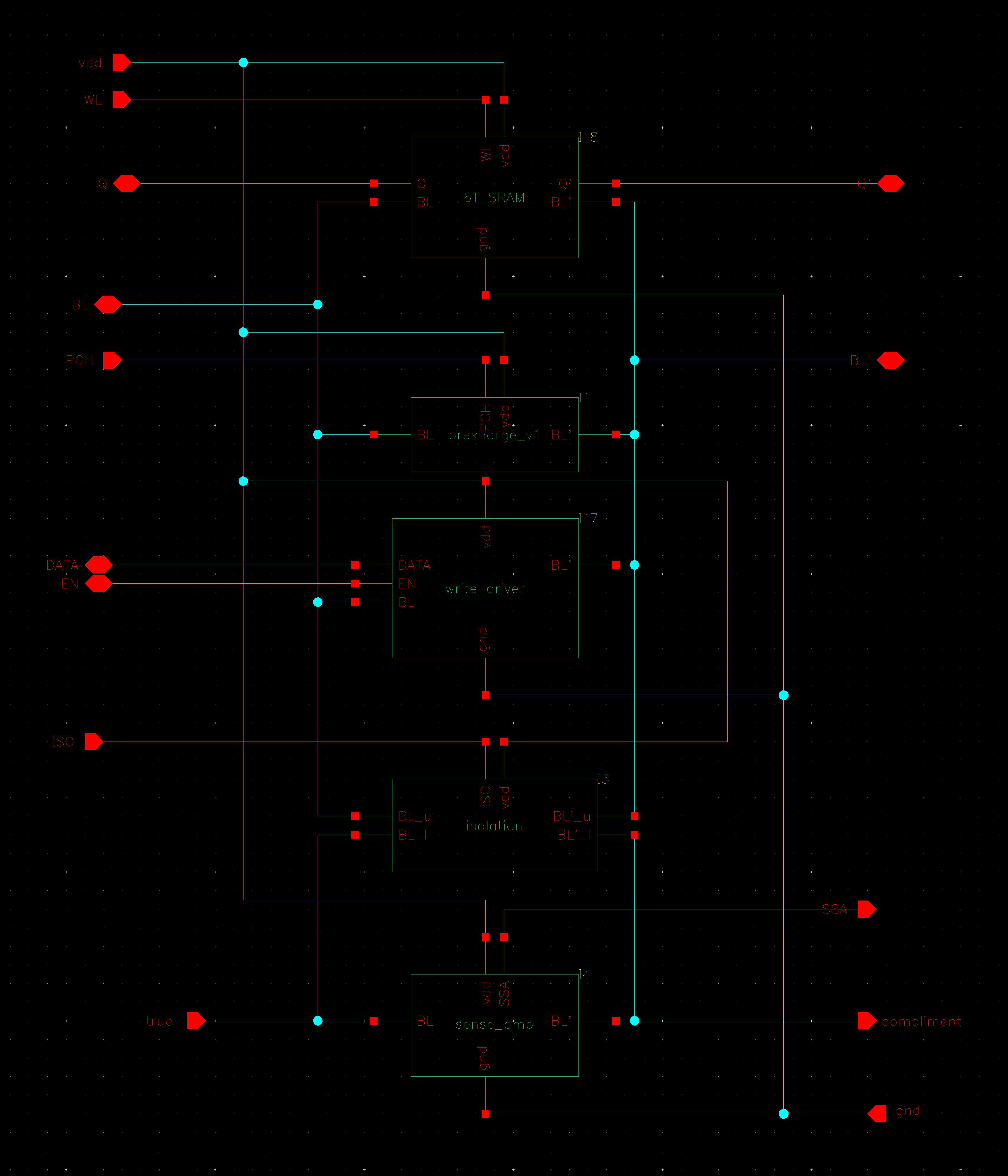
- This is the single-column SRAM block with all the peripheral devices.
In this section, presents the design methodology followed during the design of peripheral devices and the 6T SRAM cell. A brief explanation of the working of these devices has been provided wherever necessary to facilitate understanding of the design methodology
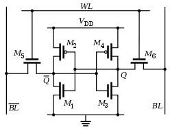
We should first understand the working of the SRAM cell and the importance of different constraints on the device sizing for read and write operations.
The following is the explanation for writing "0" logic into the SRAM which in turn emphasises the need for stronger access transistors
-
Let us consider writing a logic "0" to a cell that has stored a logic "1".
-
The write driver makes BL=0V and BL'= VDD as logic '0' is written into the cell. The write driver circuit provides the required voltage to BL and BL' ( For write 0, BL = 0, BL' = 1 and for write 1, BL=1, BL' = 0).
-
Now the corresponding address line is enabled by the decoder circuit which makes WL=1.
-
The word line ( WL ) is made high and hence bit lines BL and BL' are connected to the SRAM cell through the access transistors.
-
The corresponding data is written into the cell ( Q = 0 for write logic 0 and Q = 1 for write logic 1 ).
-
Q' side of the cell cannot be pulled high enough to ensure the writing of '1' due to the sizing constraint imposed by the read stability. It ensures that this voltage is kept below 0.4V.
-
Hence the new value of the cell has to be written through the transistor M6. Data '0' will be written into the cell if node Q is pulled down, below the threshold voltage of M1 to turn it OFF
For a successful write operation, access transistors should be stronger than the pull-up transistors which are taken care of by the pull-up ratio.
For understanding read operation, we consider the SRAM cell is holding logic "1".
- Considering, that logic "1" is stored in the SRAM cell (Q =1 and Q' = 0).
-
Initially the bit lines BL and BL' are pre-charged to VDD. Then the word line (WL) is made high. So the transistors M1, M4, M5 and M6 (Refer to above figure) will turn ON.
-
Therefore BL' gets discharged through the series transistors M5-M1 and BL will remain in its pre-charged state.
-
As the voltage difference (ΔV) between the two-bit lines builds up, the sense amplifier is activated which pulls the output level to logic "1". Therefore reading logic "1" from the cell is completed.
The key design issue for the data-read operation is to guarantee that the voltage ΔV does not exceed the threshold of M3, so that the transistor M3 remains turned OFF during the read phase.
To prevent this, the resistance of M5 should be made larger than that of M1 to prevent ΔV from turning on M3 (Not destroying the stored data). This is defined as the cell ratio.
The basic requirements which dictate the dimensions of the transistor (W/L) ratios are:
- a) The data-read operation should not destroy the stored information in the SRAM Cell i.e., Read Upset
- b) The cell should allow the modification of the stored information during the data-write phase., i.e. Write Upset.
The two most important parameters which decide the Transistor size of the SRAM cell are:
a) Cell Ratio:
- The data-read operation should not destroy the stored information in the SRAM cell. i.e. Read upset.
- The cell ratio β (beta) should be less than 1.5 for the proper functioning of SRAM cell.
The cell ratio, β for the read operation which is given by,
Cell ratio, β ={ (W\L) pull down transistors } / {(W\L) access transistor}
b) Pull-Up Ratio:
- The cell should allow the modification of the stored information during the data-write phase.
- PR should be as small as possible.(meaning access transistor M6 should be strong compared M4.)
The pull-up ratio, P.R for the write operation is given by,
Pull-up ratio, P.R ={ (W\L) pull up transistors } / {(W\L) access transistor }
These conflicting requirements for read and write operations are satisfied by sizing the bit cell transistors to provide stable read and write operations.
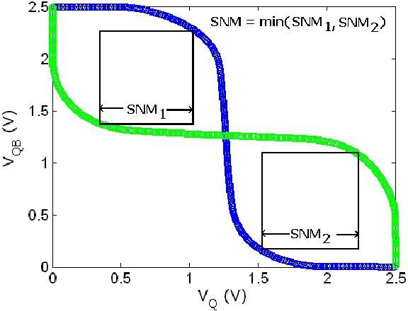
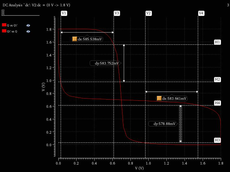
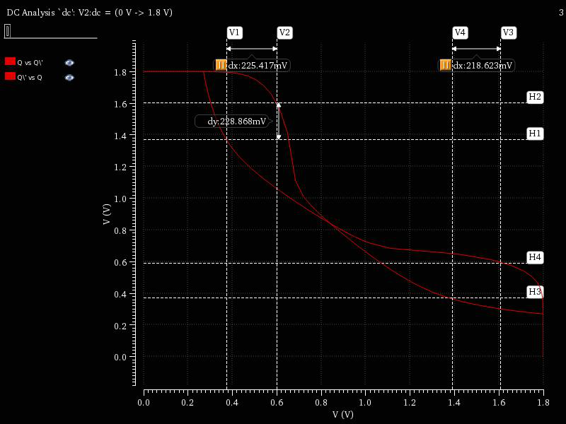
The stability of the SRAM cell can be described by the 'Butterfly curve' which is obtained by superimposing the voltage transfer curves (VTC) of the two inverters of the memory cell. The stability of the SRAM cell can be analyzed by measuring the Static Noise Margin (SNM). SNM is the measure of the stability of the SRAM cell to hold its data against noise. The Stability of the cell is given by the size of the maximum square box that can fit inside the Butterfly wing.
Butterfly curve for SRAM Cell:
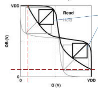
Figure: a) Butterfly curve for SRAM Cell for hold state. b) Butterfly plot for read state.
Initial condition WL=0 and Access Transistors M5 and M6 are OFF
- As access Transistors are in the OFF state the Cell is isolated from BL and BL’, Therefore there is no possibility of the state getting changed, as there will be fewer chances of Noise interference.
- If we plot the VTC of INV1 and INV2 and super-imposing the VTC's we get a butterfly curve.
- As there is no Noise getting added, the Inverters are working with a perfect VTC as shown in above figure. The Hold state Static Noise Margin (SNM) is expected to be Maximum
Consider the following READ State: WL=1, Access Transistors M5 and M6 are OFF and Bit lines are Pre-charged to VDD
- In READ, To find the SNM of the cell, we can measure the side lengths of both of noise margin squares, and the smaller of the two lengths is the SNM of the SRAM cell for read state.
- In an ideal case(no variations considered), these squares should be of equal size,and therefore only one square would need to be considered, however considering variations and transistor mismatch, these curves may not be mirror images of each other, and therefore both squares should be considered.
Key Points
- The curve flattens during a read operation, reducing the box size and thus implying reduced stability.
- The larger the box, the higher the β value and hence greater the stability.
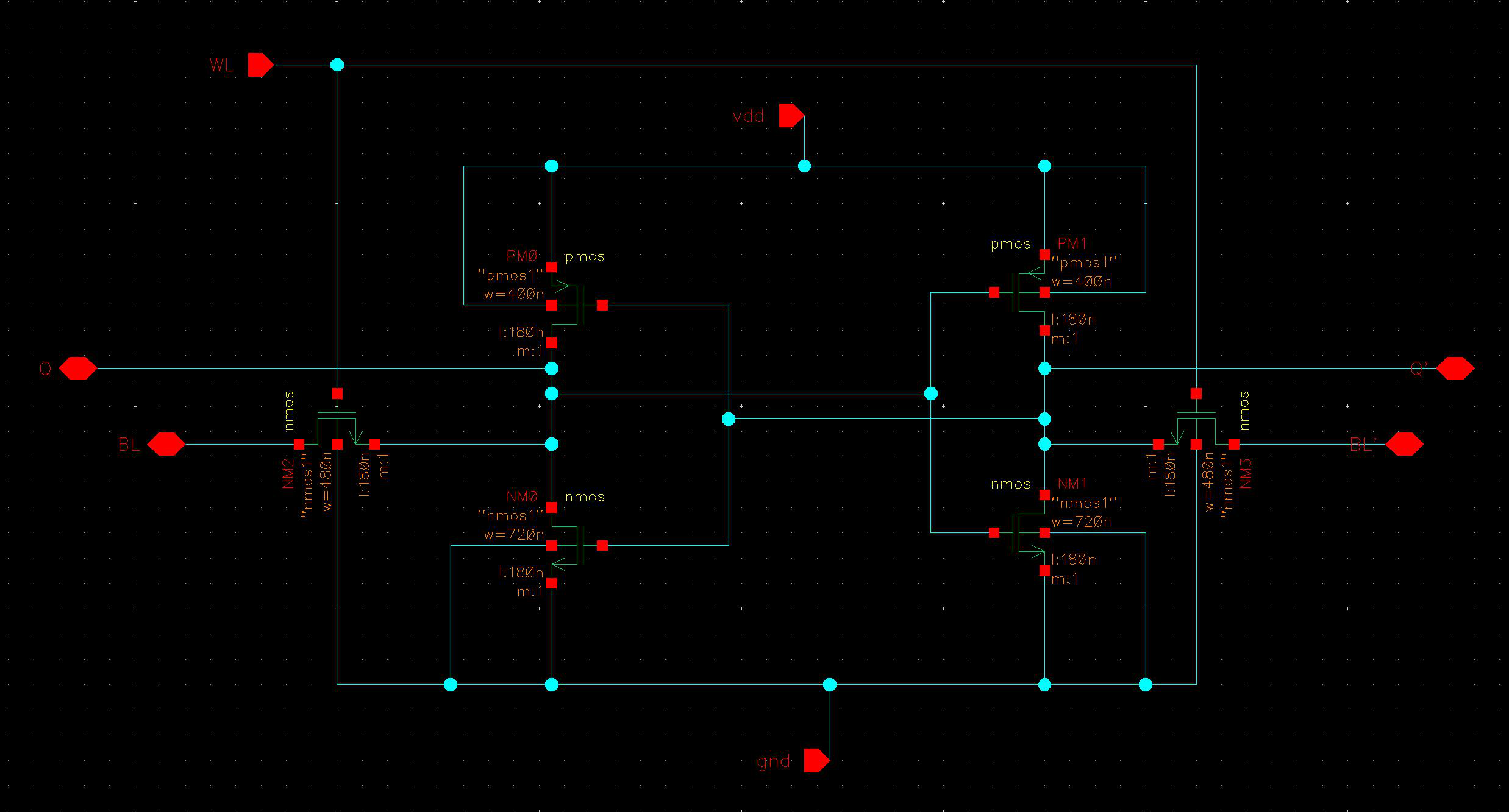
The 6T SRAM cell has been designed for the following specifications. The 6T SRAM cell is designed for a CR=1.25 and PR=0.85 for 180nm technology. To minimize area, all the transistors are sized to a minimum length i.e. 180nm. External capacitance of 120fF is connected to BL and BL' modelling the parasitic capacitance of BL and BL'
+--------------------------------+-----------------------------------+
|  **Length of all MOS**           | **180nm**                       |
+=================================+===================================+
| **Width of PMOS devices (wp)**  |  **Minimum width**               |
+--------------------------------+-----------------------------------+
|  **Access transistors width      | **1.2 x wp**                    |
|  (wa)**                          |                                 |
+---------------------------------+-----------------------------------+
| **Width of Pull down NMOS       |  **1.5 x wa**                    |
|  transistors (wn)**             |                                  |
+-----------------------------------+--------------------------------+
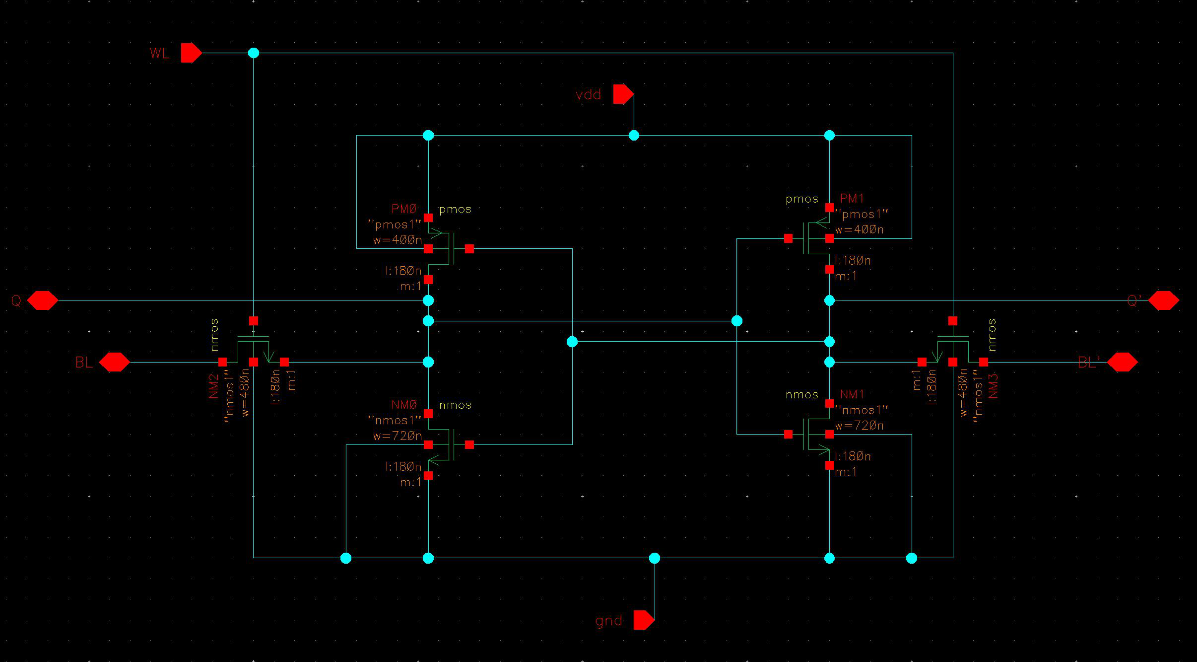
Circuit diagram of SRAM cell:
(Width of pull-up transistors Wp= 400nm, Width of access transistors Wa= 470nm, Width of pulldown transistors Wn= 590nm)
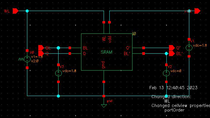
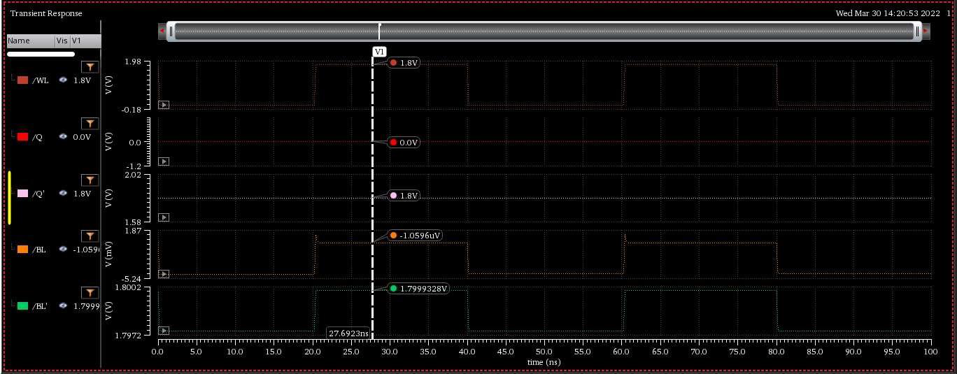
Testbench Schematic for Write "0" Operation :
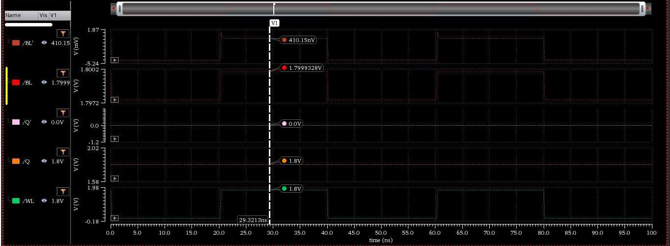
Timing diagram for Write '0' Operation:
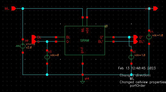
Testbench Schematic schematic for Write "1" Operation:
Timing diagram for Write "1" Operation:
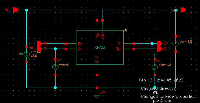
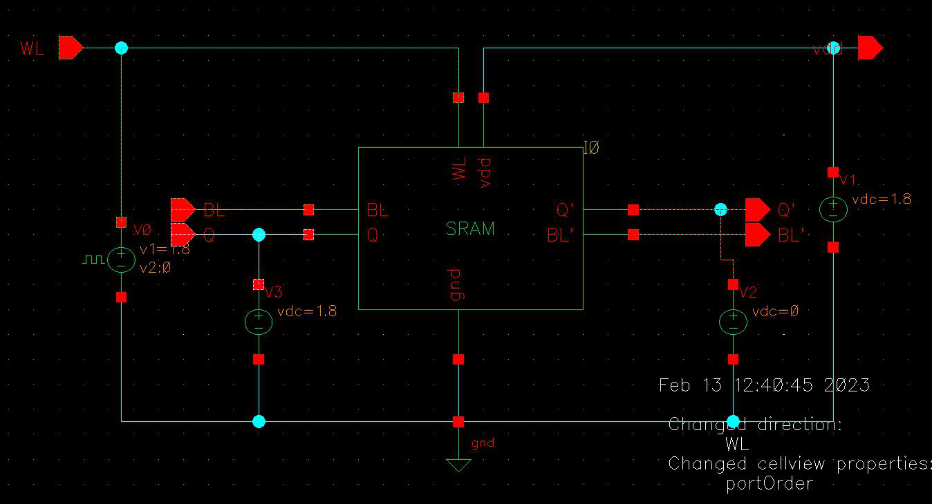
Testbench Schematic for Read "1" operation:
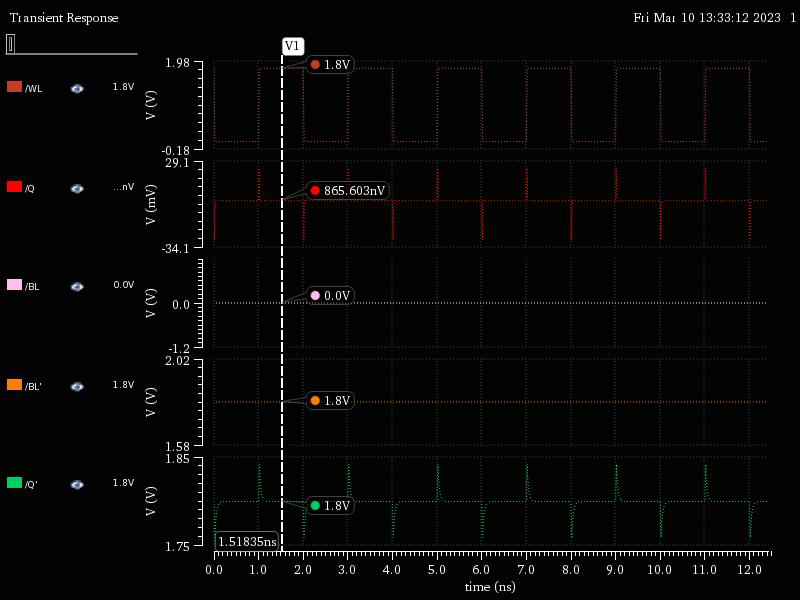
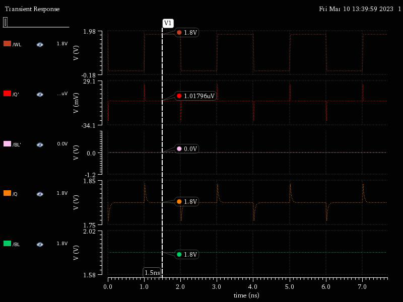
Timing diagram for Read "1" operation:
Testbench Schematic for Read "0" operation:
Timing diagram for Read "0" operation:
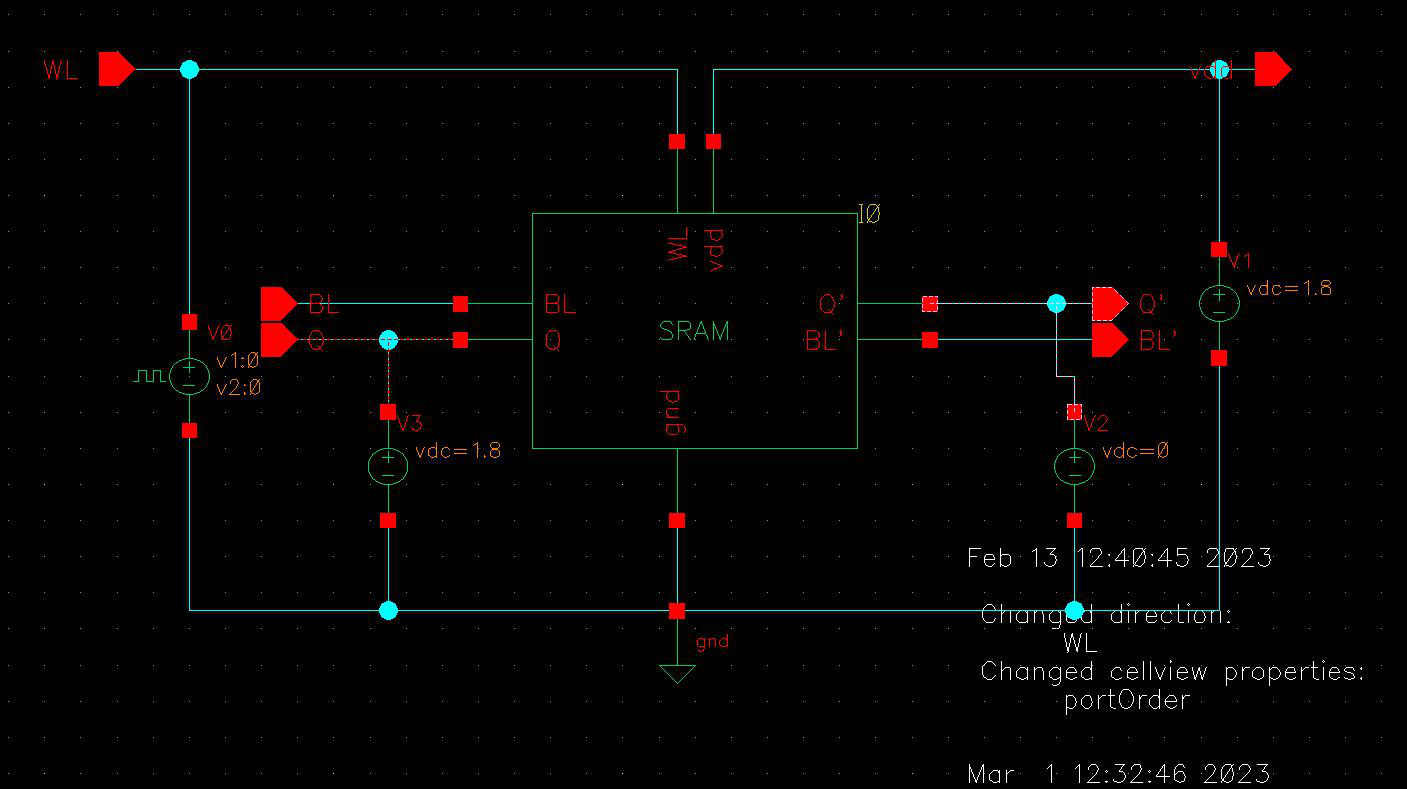
Butterfly curve for Hold state:
 SNM = min (max(SNM1),max( SNM2) )
= min (578.869mV, 585.075mV)
= 578.869mV**
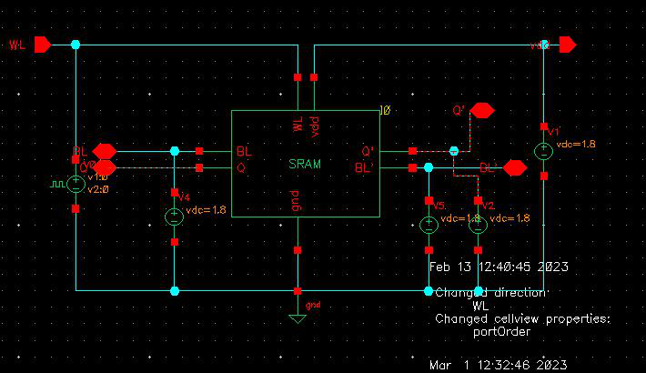
Butterfly curve for Read state
 SNM = min (max(SNM1),max( SNM2) )
 = min (225.417mV, 218.623mV)
 = 218.623 mV
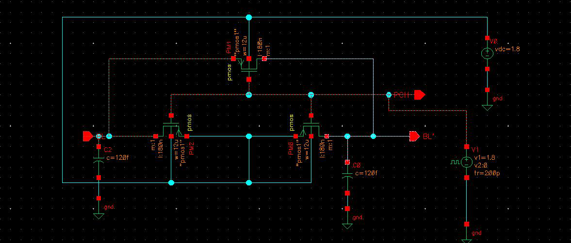
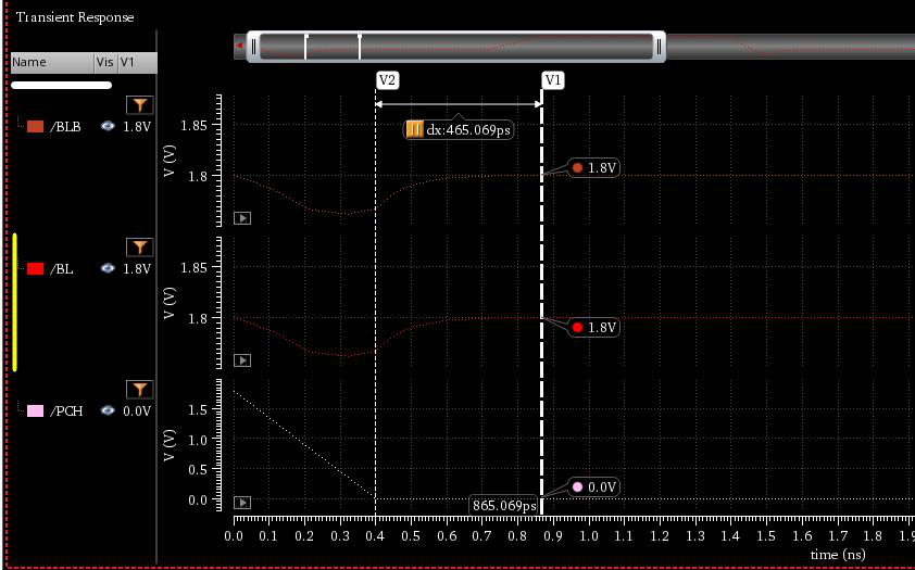
- The pre-charge circuit in this project was designed to charge a BL and BL' with the capacitance of 120f with minimal charge time. in 0.5n Seconds
Testbench schematic for Pre-charge circuit:
(Width of the transistors = 12um)
The timing diagram for the precharge circuit :
The write driver circuit was designed to have minimal latency.
Timing diagram which is a simulation to find the time taken to generate the data to be written on BL and BL' and check the latency of the write driver circuit.
The circuit took 0.5249ns to generate the data to be written i.e to produce the voltage difference on BL and BL'
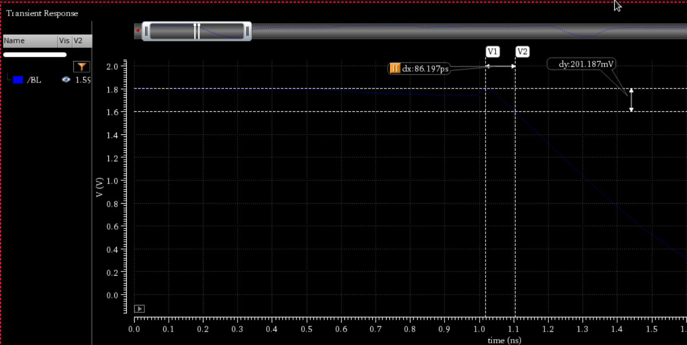
The simulation was conducted for read operation to find the time it takes to sense 200 mV sense margin ( difference in voltage between BL and BL' after WL is made HIGH )
The circuit took 86.17ps to sense the 200mV sense margin.
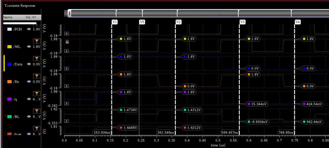
Schematic of SRAM Architecture with all the peripheral devices connected.
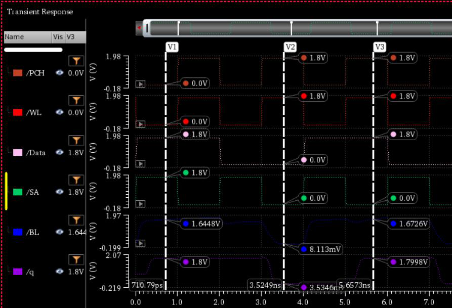
The timing diagram for SRAM Architecture for Wrtie logic "1" operation followed by read logic "1" and write logic "0" followed by read logic "0".
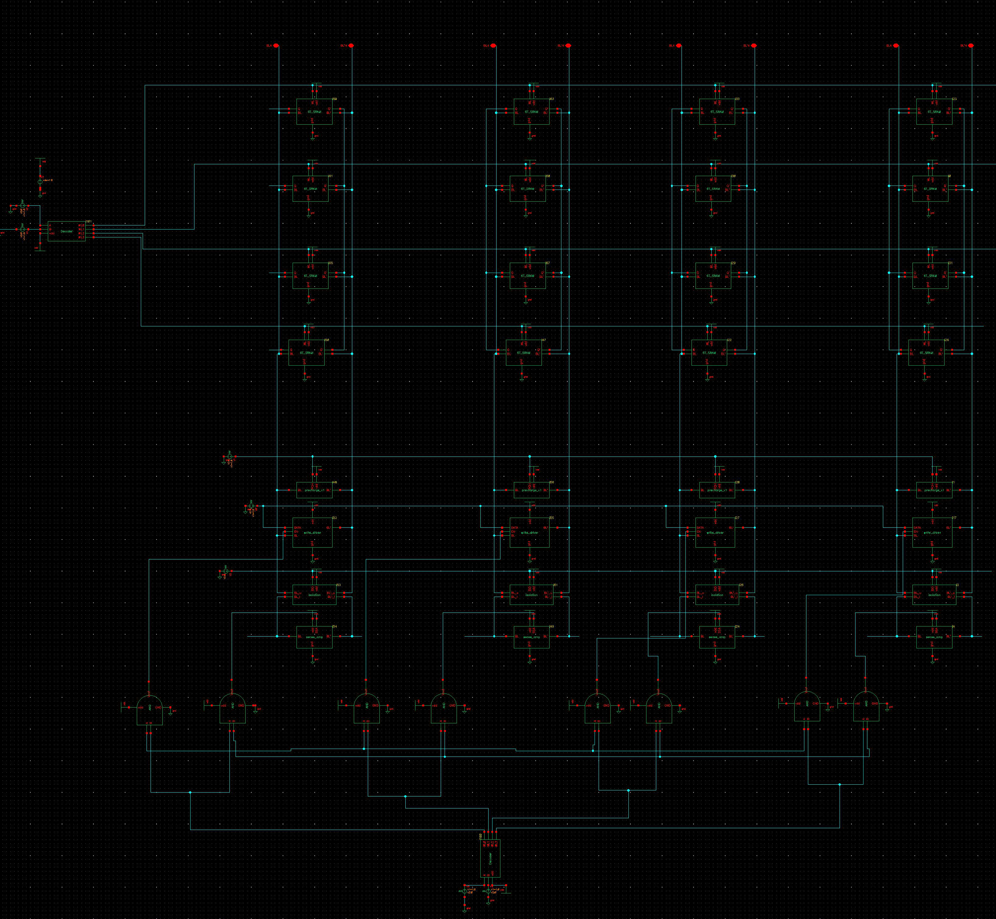
A 4X4 memory array (16-bit memory array) was designed and simulations were performed for write and read operations on the memory array
Schematic of the 4X4 memory array:
Addition circuits column decoder, row decoder and row enable circuits were designed and added.
-------- work in progress -----------
Through this project, we have learnt how to design, simulate, and analyse the SRAM Architecture { 6T SRAM cell, Pre-charge circuit, Isolation Circuit, Sense amplifier and Write driver circuit) working on GPDK 180 nm technology using Cadence tool-chain. We have analysed the Static Noise margins, and latency for peripheral circuits. Finally, a 4x4 Memory array was designed and simulations were performed. The project has captured enough details of the entire design, test, and simulation phase and meets its project objective.
I hope this project helps explorers to accelerate their exploration around SRAM design. I hope to contribute more such repositories which aims not only to achieve the defined design objectives but also to foster a collaborative environment for knowledge sharing and continuous improvements.
Please feel free to explore the repository, contribute, raise issues, and engage in discussions as we work together to achieve the project goals.
I would like to express my sincere gratitude to Prof. Mahesh Awati for his exceptional teaching and guidance throughout the course. His support and assistance with all the lab work have been invaluable. Also, I would like to thank PES University for providing us with all the necessary infrastructure.


