EN | 中文
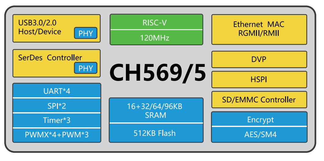
CH569 and CH565 are based on RISC-V3A core, and support the IMAC subset of RISC-V instructions. The chip integrates super-high-speed USB3.0 host and device controller (built-in PHY), Gigabit Ethernet controller, dedicated high-speed SerDes controller (built-in PHY, can drive optical fiber directly), high-speed parallel interface (HSPI), digital video port (DVP), SD/EMMC interface controller and encryption/decryption module. The DMA with width of 128 bits can ensure high-speed transfer of large amounts of data. CH569/CH565 can be widely used in streaming media, instant storage, super-high-speed USB3.0 FIFO, communication extension, security monitor and other applications.
- RISC-V core, 120MHz system clock frequency. Single-cycle multiplication and hardware division. Programmable interrupt controller. Low-power two-stage pipeline;
- 448KB Code Flash, 32KB DataFlash, 16KB SRAM with width of 32 bits, 32/64/96KB configurable SRAM with width of 128 bits;
- Built-in super-high-speed USB3.0 controller and transceiver (built-in PHY). USB3.0 Host/Device mode. OTG capability. Support USB3.0 HUB;
- Built-in high-speed USB2.0 controller and transceiver (built-in PHY). USB2.0 Host/Device mode. Control/bulk/interrupt/synchronous transfer;
- Built-in gigabit Ethernet controller (Ethernet). Provide RGMII and RMII PHY interface. 10/100/1000Mbps transfer rate;
- Built-in digital video port (DVP). Data width can be configured as 8/10/12 bits. Support YUV, RGB, JPEG compressed data;
- Built-in high-speed parallel interface (HSPI). Data width can be configured as 8/16/32 bits. Built-in FIFO. DMA capability. The maximum transfer speed can reach around 3.8Gbps;
- Built-in SerDes controller and transceiver (built-in PHY, can drive optical fiber directly). Support network cable transfer distance of 90 meters (only use one set of differential line). Support 1.25Gbps high-speed differential signal communication;
- Built-in EMMC controller. Support single-wire/4-wire/8-wire data communication mode. Comply to EMMC Specification Rev. 4.4 and Rev. 4.5.1, compatible with Specification Rev. 5.0;
- Support AES/SM4 algorithm. 8 types of combinations for encryption/decryption modes. Support encryption/decryption of SRAM/EMMC/HSPI data;
- 4 UARTs. Baud rate can be up to 6Mbps. Compatible with 16C550. Built-in FIFO. Multiple trigger levels;
- 2 SPIs. Master/Slave mode. Built-in FIFO. DMA capability;
- Active parallel port: 8-bit data, 15-bit address bus;
- 3 x 26-bit timers. Support timing, count, signal capture, PWM output, 4 expanded PWM outputs. Adjustable duty cycle;
- 49 general-purpose IOs. 8 settable level/edge interrupts. Some pins have alternate and map functions;
- Built-in watchdog, which integrates 2-wire debug interface and supports emulate online;
- Low-power mode. Support wake up some GPIOs, USB and Ethernet signal;
- Chip ID: unique 64-bit ID;
- Package: QFN68, QFN40.
