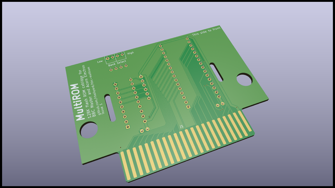
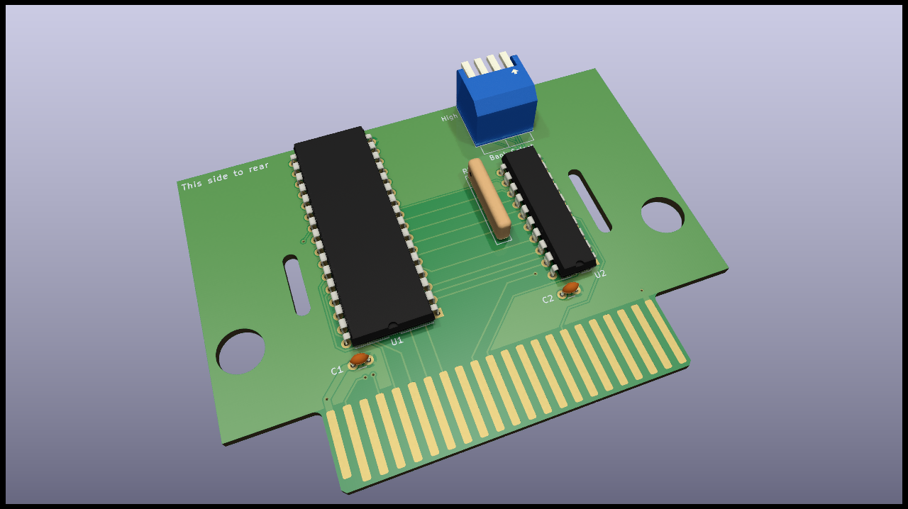
There are plenty of perfectly-good options for building ROM cartridges for the BBC Master and Acorn Electron Plus One. However, I am a stubborn git and enjoy reinventing the wheel for fun, so I decided to come up with my own take on the concept.
Rather than use the 27x and 28x series (E)EPROMS that were used Back In The Day, MultiROM uses a NOR Flash IC, the SST39SF010A. This part is much cheaper and more readily available than EEPROMs, but can still be obtained as a through-hole part for easy DIY assembly. Additionally, it offers more capacity (a whopping one megabit!), which MultiROM uses to store multiple ROM images on one cartridge, selected by DIP switches.
The schematic and PCB layout were produced using KiCad 7.0.
| Reference | Part |
|---|---|
C1, C2 |
Ceramic capacitor, 0.1μF |
RN1 |
SIP6 resistor network, bussed, 10KΩ |
SW1 |
SPST DIP switch module, 4 switches |
U1 |
SST39SF010 1Mbit flash memory, DIP32 package |
U2 |
GAL16V8 or ATF16V8 programmable logic device, DIP20 package |
RN1 can be omitted if you trust the weak pull-ups built into U2. I forgot to order it when building my prototypes, and they seem to work just fine without it.
SW1 can be omitted if you want the cartridge to function as a basic 2x16k catridge without bank switching.
Any PCB fabricator service such as PCBWay, OSHPark or JLCPCB should be able to fabricate the board. Some shops will accept the .kicad_pcb file directly, but most will require Gerber and drill files. These can be exported from Kicad using the File -> Fabrication Outputs menu options.
Ideally, the edge connector should have a chamfered board edge and hard gold-plated contacts, to avoid damaging the PCB socket and to ensure a good connection. These are usually extra-cost options that have to be requested when placing the order.
When assembling components onto the PCB, pay attention to which side they are on! Integrated Circuits U1 and U2 go on the back side of the PCB, with their orientation notches facing towards the edge connector.
This project uses KiBot to automate output in various formats from KiCad; release archives contain manufacturing files for various popular PCB fabricators.
U2 is a programmable GAL that provides selection and addressing logic compatible with both the Electron and BBC Master.
GALasm source for U2 can be found in the pld/ directory, see the README in that folder for instructions on building and programming.
The MultiROM PCB is designed to fit in the 'standard' Master/Electron cartridge case produced by Acorn. I do not have a real cartridge to check this against, but I 3D-printed Paul Boddie's OpenSCAD cartridge and it fits nicely in there.
If the bank-selection DIP switches (SW1) are installed, a suitable cutout will need to be made in the case.
Note that there is very little clearance for components inside the case - if the board is to fit inside the case, then the ICs must be soldered directly onto the board rather than socketed.
With the machine powered off, insert MultiROM into either the front or rear cartridge slot. In the rear slot, MultiROM will appear as Sideways ROMs 0 and 1. In the front slot, it will appear as Sideways ROMs 2 and 3.
Keep in mind that the cartridge housing is the only thing preventing a cartridge from being inserted backwards! If using a bare MultiROM board, pay attention to the "This side to front" markings - the correct orientation is with the chips facing away from you.
Each cartridge slot corresponds to two Sideways ROMs - 0 and 1 for the rear cartridge slot, and 2 and 3 for the front. The DIP switch SW1 on the front of the cartridge allows one of four banks to be selected for each ROM, allowing multiple ROM images to be stored on the cartridge.
The left two switches select the bank for ROM 0 or 2, the right two switches select the bank for ROM 1 or 3.
While switching banks on a running machine is unlikely to cause any permanent harm, it will almost certainly cause the machine to crash the next time a ROM service call is issued. Always reset the machine after switching banks!
The tools/ directory contains software suitable for either a Master or Electron, that can program MultiROM, query Sideways ROM slots, and save Sideways ROMs to tape or disc.
Source is in BeebASM format.
The flash IC can be programmed in an external programmer according to the following memory map.
| Address Range | ROM | Bank |
|---|---|---|
| 00000-03FFF | Low | 0 |
| 04000-07FFF | High | 0 |
| 08000-0BFFF | Low | 1 |
| 0C000-0FFFF | High | 1 |
| 10000-13FFF | Low | 2 |
| 14000-17FFF | High | 2 |
| 18000-1BFFF | Low | 3 |
| 1C000-1FFFF | High | 3 |
The SST39SF010A is flash memory, and cannot be programmed like a regular EEPROM. Data can only be erased in 4kb sectors, and writes and erase operations are performed using command strings written to 'magic' addresses. Writes can only be made to erased memory. After issuing an erase or write command, the chip must be allowed to complete the operation before continuing.
Completion can be determined by repeatedly reading back the written byte - until the operation is complete, bit 7 will be inverted, and bit 6 will toggle with each subsequent read.
Since the programming process is so convoluted, and regular writes are ignored, a write protection jumper is not provided.
Writing, erasing, chip-status and chip-ID functions are accessed by performing a 'magic' sequence of writes, as described in the datasheet, to addresses 5555 and 2AAA
Because the cartridge slots are mapped into memory starting at address &8000, and the low/high ROM select line is used as the 14th address bit, when programming flash on the machine, use the following addresses:
| Flash address | ROM | BBC Address |
|---|---|---|
5555 |
1 / 3 | 9555 |
2AAA |
0 / 2 | AAAA |
E.g., to write a byte to ROM 0 (i.e. the low ROM in the front cartridge socket), assuming that the sector has been erased:
- Page in ROM 1
- Write
&AAto&9555 - Page in ROM 0
- Write
&55to&AAAA - Page in ROM 1
- Write
&A0to&9555 - Page in ROM 0
- Write a byte to the desired address
- Repeatedly read back any ROM address until two consecutive reads yield the same data.
This process must be repeated for each byte.
Any spurious reads or writes occurring during this process will cancel the operation or cause undesirable effects - to prevent MOS from interfering it is advisable to disable IRQ interrupts with an SEI instruction.
tools/flashio.6502 contains utility routines for erasing and programming the flash, and safely querying its ID bytes without corrupting Sideways RAM. These were written for use by the tools in that directory, but are heavily commented and designed to be reused.
-
Modify Paul Boddie's OpenSCAD cartridge case to have a cutout for the DIP switches (and maybe cutouts for IC sockets too?).
-
Recruit a volunteer to test cartridge and software functionality on Electron.
-
Phillip Pearson's Electron flash cartridge - uses SST39SF010A, but can't be written on a Master, and does not have bank switching.
-
Stardot thread for Retro Hardware ARA III - writeable cartridge that uses a GAL to support both Electron and Master, but uses expensive 28C256 EEPROM.
-
BooBip.com Sideways Flash Module - another SST39SF010A-based ROM replacement, designed to plug into internal Sideways ROM sockets.
-
Acorn Application Note 014: Acorn Electron Cartridge Interface Specification - Official cartridge interface specs, including differences between Electron and Master.
-
BeebWiki article on Sideways ROM - especially the section on the Electron and its ROM-selection quirks. See also, this Stardot post with a technical background on the Electron's ROM selection register.

