In these exercise sessions, you will develop a complete microprocessor in Verilog. You start by assembling the necessary components to a single cycle processor and run a simple program on it. Next, you will increase the performance, by pipelining the processor. The main objective of this lab session is ensuring the functionality of our CPU as well as to understand its performance and necessary hardware resources. The processor will be synthesized in a 32 nm CMOS technology using generic libraries from Synopsis using regular Vt Cells. The clock frequency used for synthesis is 10 MHz, which means a clock period equals to 100 ns.
In order to complete your assignment, you will work with a set of tools. These tools are set up for you, but they are also very typical tools used in industrial digital design. The performance of the processor will be evaluated through cycle-accurate simulation using NC Verilog. Through the use of synthesis tools from Design Vision, the hardware resources needed for its implementation will be evaluated.
To create your workspace you have two options:
- Fork the repository with the starting material from GitHub (see below) and use git as versioning tool of the development of the project (suggested).
- Download from Toledo the file processor_design.zip located in the folder Exercise Sessions. Extract it to some location of your system. The folders that compose our project workspace are:
- tools_scripts: Scripts for running the tools used during the exercises.
- RTL: All the Verilog files that define the logic of the processor.
- SIM: Files for running the simulation of the HDL code.
- SIM/data: Subfolder that contains the assembly code to run.
- SYNTHESIS: Files for running the synthesis of the processor. For using the tools and completing the exercise sessions you need to access through SSH connection to a virtual workspace on the ESAT servers. Login details are available on the dedicated startup SSH guide.
If you are not familiar with SSH connections and/or git versioning tool, please check out the documents and guides provided for you in the course material.
To run the simulation of the processor:
- Run the tool script going to the folder tools_scripts. Run the command
source incisiv_15.20.058.rc - Go to the folder SIM. Run the command
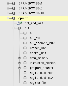
make nc_guithrough a terminal (Optionally run the commandmake ncto use the tool without graphical interface which checks the correctness of the program). This command will call all the hdl files declared inSIM/files_verilog.fand will execute the testbenchRTL/cpu_tb.v. This testbench (1) declares an instance of the cpu (2) loads the instruction memory from the fileSIM/data/imem_content.txt(3) loads the data memory from the fileSIM/data/dmem_content.txt(4) Starts the execution of the instructions. - After running the command, the NC verilog graphical interface will open. In the left part of the window the whole hierarchy of the design could be found. With the objective of displaying the internal signals for debugging go to the target submodule and select it. Afterwards do right-click over the signals to display and select “Send to Waveform Window”. Finally run the simulation with the button:

To synthesize your verilog code into a netlist which can be used for area and power simulations:
- Run the tool script going to the folder
tools_scripts. Run the command:source synopsys_2017.09.rc - Go to the folder
SYNTHESIS. Run the synthesis through the command:source synthesis.shThis command will load the libraries from the technology (standard cells, memory macros, etc) as well as the design constrains through the sdc file:SYNTHESIS/design_constraints.sdc(This file defines specifications from the designer such as the frequency, false paths, etc).
The netlist obtained through this process could be found in the folderSYNTHESIS/gate/cpu.v. The reports of area, power, resources and timing are generated in the folderSYNTHESIS/rep.
- The datapath as well as its submodules have been already implemented for you in Verilog. However, the functionality of the processor must be completed by carrying out the tasks described underneath.
- The assignments must be completed in groups of 2 people.
- After completing each one of the exercises the results must be shown to the TAs for its correspondent evaluation.
- The code must be delivered to the TAs in the final session.
- Also, you will hand in a small report based on the questions you find on the last page. Together with the performance of your final processor, this counts for 2 points in the final H05d3A grade. This report is handed in through Toledo. The deadline will be set and communicated to you.
Complete the internals of the control unit to handle the following instructions: (BEQ, JUMP, LW, SW, ADDI as well as R-type ALU instructions called ‘ ALU_R’). Set the outputs of the control unit correctly depending on the fetched instruction, ensure the correct datapath behavior.
- → For debugging purposes, you can use the test code simple_program contained in the folder SIM/data, containing all the supported instructions interleaved by NOP instructions. Next, the code “MULT1” executes the multiplication of 5 integers and sum all the results. Test this code to ensure that your design is correctly implemented.
- → After obtaining a functional model run the synthesis.
The processor completed in the last exercise is able to execute multiplications through sums and shifting since there is no hardware support to carry out the multiplication in one cycle. With the purpose of boosting performance, your task will be to add hardware support for multiplication and evaluating its impact on performance, area and timing. The processor must be able to process the multiplication instruction MULT. The format of the instruction is the following:
| [31:26] Opcode | [25:21] source reg 1 | [20:16] source reg 2 | [15:11] destination reg | [5:0] function Field |
|---|---|---|---|---|
| 000000 | XXXXX | XXXXX | XXXXX | 011000 |
Three files might need to be modified for this purpose: control.unit.v, alu_control.v and alu.v. To test the performance and correctness of your design, load the assembly test code “MULT2” which uses now the implemented MULT instruction to carry out the same 5 multiplications and sums of the testcode “MULT1”. After updating your design, run the simulation and synthesis again.
Is it necessary to modify the control unit for the insertion of the MULT instruction?
In this part of the session we will modify our processor to convert it to a pipelined implementation. For the following exercises assume data and control hazards are solved by NOP instructions.
For a processor with 5 pipelined stages (Instruction Fetch (IF), Instruction Decode (ID), Execute (EXE), Memory (MEM) and Write Back (WB)), identify which hardware resources belong to each of the mentioned stages, and which signals should go from stage to stage. Try to match the HDL code with the Architecture, and complete the tables underneath (you can complete directly in the readme.md file if you want).
| IF | ID | EXE | MEM | WB | |
|---|---|---|---|---|---|
| Datapath Resources | |||||
| IF → ID | ID → EXE | EXE → MEM | MEM → WB | |
|---|---|---|---|---|
| Signals | ||||
Insert the pipelined registers where necessary, using the module reg_arstn_en.
reg_arstn_en #(.DATA_W(16)) signal_pipe_ID_EX(
      .clk   (clk       ),
      .arst_n(arst_n    ),
      .din   (signal_IF  ),
      .en    (enable    ),
      .dout  (signal_ID)
   );
This module implements a register with variable width, which is set through the parameter DATA_W. See the inset on the right for an example for such a pipelined register between the Fetching (signals signal_IF) and Decode stage (signal_ID). Connect the enable signal of the pipelined registers to the global enable signal called enable. After updating your design, run the test code MULT2 and ensure the correct functionality. Finally, run the synthesis scripts.
Since the pipelined processor implemented does not have support for handling data hazards, the execution of more complex code containing branches or data dependencies would not work properly. Add hardware support for forwarding and stalling in order to achieve this functionality. Run synthesis, and compare the results with previous implementations. After updating your design, run the test code MULT3 and ensure the correct functionality. Finally, run the synthesis scripts
Now that you know how a processor work you can implement “from scratch” another ISA.
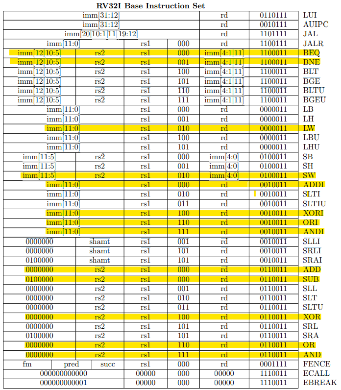
Available online it is possible to find the official technical specification for the RISC-V Instruction Set Architectures. As RISC-V was designed for flexibility and modularity, there are different base versions and extensions that one can choose to support in hardware. We will use only part of the RV32I Base Integer Instruction Set (described in Chapter 2 pp 13-30) but in the document you can have a look at all the others. For this part of the project you need to write the Verilog code (or change the one you used so far) for the instructions highlighted below (you can use either the single cycle or the pipelined version). You can also find the list at page 130 of the specifications.
Is anything missing in the list? How do you implement the NOP and STOP instructions?
HINT: use the files in this repo as a reference, keep the same file names for testing and synthesis
Now that you designed the core you need to test every supported instruction. The idea is to use the same testing environment provided in the exercise’s material for a simple program. Of course, you need to write a new instruction memory input file, which contains RISC-V binaries. If you rename your files as explained in the simulation guide above, the verification will start and check only few instructions. If you open the cpu_tb.v file in the RTL directory, searching for the test_basic task, you will see how such basic test is done; try to understand it and add the testing of all the instruction you need to support. (HINT: it is important that the destination registers you set in the instructions is coherent with the one you check in the testbench. Change input data memory state if required.) After fully checking your design run the synthesis. Is it any better from the MIPS core?